My Report about PIC16F84A Microcontroller Implementation on Verilog Hardware Description Language23/3/2021 NoteThis is one of my Doctoral assignment from Advanced Computer Architecture II Course which has never been published anywhere and I, as the author and copyright holder, license this assignment customized CC-BY-SA where anyone can share, copy, republish, and sell on condition to state my name as the author and notify that the original and open version available here. 1. IntroductionPeripheral interface controller (PIC) is a family of microcontrollers made by Microchip Technology. A microcontroller is a one chip computer that include microprocessors, memories, and peripherals. PIC devices are popular with both industrial developers and hobbyists due to their low cost, wide availability, large user base, extensive collection of application notes, availability of low cost or free development tools, serial programming, and re-programmable Flash-memory capability. They can be programmed to be timers, to control a production line, to control light and sound intensity by involving few sensors, and to perform other kind of tasks. The PIC microcontroller have five basic instruction cycle which are fetch, decode, execute, memory, and write (FDEMW) . [1] 2. Verilog HDL Design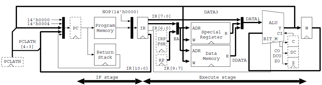
On the verilog hardware description language (HDL) design is based on Figure 1. This sections starts by constructing the arithmetic logic unit (ALU), bitmask, and W register. Then continue to design the program counter and return stack which its values to be sent to the instruction register where there is also decode and control behavior. Next is the design of special register, although the effective addressing is discussed in early part. After that the built module have to be connected to the firstly created ALU, bitmask, and W register. Lastly implement sleep and tristate buffer. 2.1 Arithmetic Logic Unit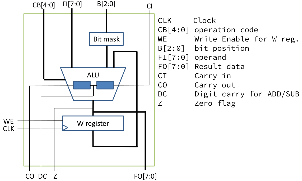
Code 1. Input and output of ALU module alu ( CLK, CB, WE, B, FI, FO, CI, CO, DC, Z ); input CLK;// Clock input [4:0] CB; // operation code input WE; // Write enable for W register input [2:0] B; // bit position input [7:0] FI; // operand input CI; // Carry in output [7:0] FO; // dest bus output CO; // Carry out output DC; // Half carry output Z; // Zero reg HC; // half carry reg [7:0] W; reg [8:0] tmp; reg [7:0] bit_mask; wire sub; assign sub = ( CB == `ISUB ); Code 2. Bitmask always @( B ) case( B ) 3'b000: bit_mask = 8'b0000_0001; 3'b001: bit_mask = 8'b0000_0010; 3'b010: bit_mask = 8'b0000_0100; 3'b011: bit_mask = 8'b0000_1000; 3'b100: bit_mask = 8'b0001_0000; 3'b101: bit_mask = 8'b0010_0000; 3'b110: bit_mask = 8'b0100_0000; 3'b111: bit_mask = 8'b1000_0000; default: bit_mask = 8'bxxxx_xxxx; endcase 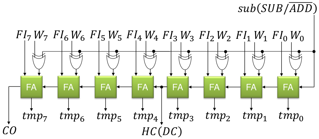
Code 3. Up to add and sub always @( CB or FI or W or HC or CI or bit_mask or sub ) begin HC = 1'b0; casex( CB ) ` IPSW: tmp = { 1'b0, W }; // Pass W register value `ICLR: tmp = 9'b0_0000_0000; // Clear `IADD, `ISUB: begin { HC, tmp[3:0] }= {1'b0,FI[3:0]} + {1'b0, sub? ~W[3:0]:W[3:0]} + sub; tmp[8:4] = {1'b0,FI[7:4]} + {1'b0, sub? ~W[7:4]:W[7:4]} + HC; end The verilog design of the ALU is based on the diagram on Figure 2. The input, output, and process looks clear which was implemented on Code 1, however the detail operation within the bitmask, ALU, and w register should be examined on Code 2, Code 3, and Code 4. The ALU operates between the value on the W register and the current input FI. For addition and subtraction, Code 3 should follow the diagram on Figure 3, while for other operations are not as complicated which is on Code 4. After that, the output can be written on Code 5. The operation definitions are available on Code 6 which the bit opcode from 2nd to 6th from left to right is used. Code 4. Other Operations `IDEC1, `IDEC2: tmp = { 1'b0, FI } - 1 ; // Decrement, Decrement and skip if 0 `IOR : tmp = { 1'b0, FI } | { 1'b0, W } ; // Logical OR `IAND: tmp = { 1'b0, FI } & { 1'b0, W } ; // Logical AND `IXOR: tmp = { 1'b0, FI } ^ { 1'b0, W } ; // Logical Exclusive OR `IPSF: tmp = { 1'b0, FI } ; // Pass FI `INTF: tmp = { 1'b0, ~FI } ; // Complement FI `IINC1, `IINC2: tmp = { 1'b0, FI } + 1 ; // Increment, Increment and skip if 0 `IRRF: tmp = {FI[0], CI, FI[7:1]} ; // Rotate Right through Carry `IRLF: tmp = {FI, CI} ; // Rotate Left through Carry `ISWP: tmp = {1'b0, FI[3:0], FI[7:4]}; // nibble swap `IBCF: tmp = {1'b0, FI} & {1'b0,~bit_mask} ; // bit clear `IBSF: tmp = {1'b0, FI} | {1'b0, bit_mask} ; // bit set `IBTF: tmp = {1'b0, FI} & {1'b0, bit_mask} ; // bit test default: tmp = 9'bx_xxxx_xxxx; end case end Code 5. Output, W Register, and Flags // FO assign FO = tmp[7:0] ; // W Register always @( posedge CLK ) if( WE ) W <= tmp[7:0] ; // Flag assign CO = tmp[8] ; // Carry Borrow flag assign DC = HC ; // Half carry flag assign Z = (tmp[7:0] == 0) ; // Zero flag endmodule Code 6. ALU Operation Definition `define IPSW 5'b00000 // Pass W `define ICLR 5'b00001 // Clear `define ISUB 5'b00010 // Sub `define IDEC1 5'b00011 // Dec `define IOR 5'b00100 // Or `define IAND 5'b00101 // And `define IXOR 5'b00110 // Xor `define IADD 5'b00111 // Add `define IPSF 5'b01000 // Pass F `define INTF 5'b01001 // Not `define IINC1 5'b01010 // Inc `define IDEC2 5'b01011 // Dec `define IRRF 5'b01100 // Rotate Right with carry `define IRLF 5'b01101 // Rotate Left with carry `define ISWP 5'b01110 // Nibble swap `define IINC2 5'b01111 // Inc `define IBCF 5'b100?? // Bit Clear F `define IBSF 5'b101?? // Bit Set F `define IBTF 5'b11??? // Bit Test F 2.2 Core Input, Output, and Register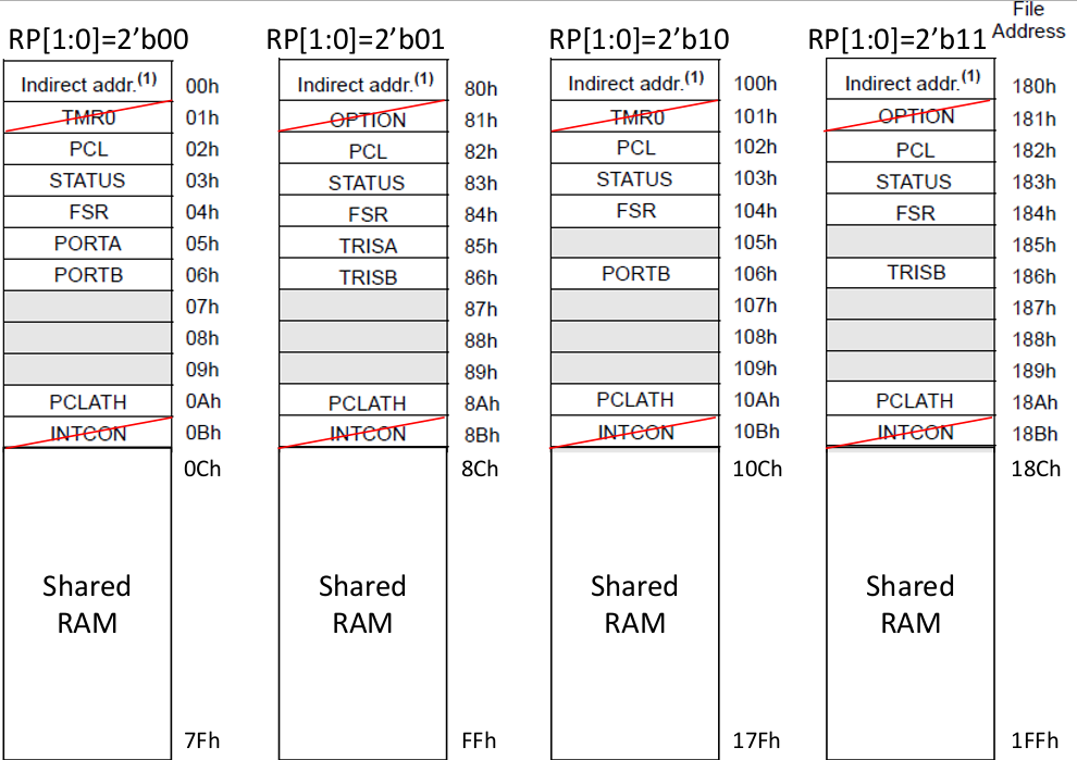
Code 7. Input, Output, and Register for Core Module // STATUS Register `define STATUS { IRP, RP, nTO, nPD, Z, DC, C } // IR `define IRB IR[ 9:7] `define IRK IR[ 7:0] `define IRF IR[ 6:0] `define IRA IR[10:0] // Memory Address `define A_INDF 7'b000_0000 `define A_PCL 7'b000_0010 module pic16core ( CLK, RST, RA, RB ); input CLK; input RST; inout [7:0] RA; inout [7:0] RB; parameter PROG = "program.mem"; // Special Register reg IRP; reg [1:0] RP; reg nTO, nPD, Z, DC, C; // 03 83 // STATUS reg [7:0] FSR; // 04 84 reg [7:0] PORTA, TRISA; // 05 85 reg [7:0] PORTB, TRISB; // 06 86 reg [4:0] PCLATH; // 0A 8A reg [7:0] RAM[ 12 : 127 ]; // 0C-7F // DATA bus reg [7:0] SDATA; // for special register reg [7:0] RDATA; // for ALU operand wire [7:0] WDATA; // for ALU result wire [7:0] DDATA; // for Data RAM Read Data // Flag data from ALU to Flag register wire CO, DCO, ZO; // Control Signal reg NOP_S; // Fetch cancel on CALL, GOTO reg [4:0] ALU_CB; // ALU control reg W_W; // Write enable for W register reg C_W, DC_W, Z_W; // Write enable for Flag register (STATUS[2:0]) reg F_W; // Write enable for Data memory reg WDT_C; // WDT clear reg nTO_S, nTO_C; // nTO set and clear reg nPD_S, nPD_C; // nPD set and clear reg SLEEP; // Sleep mode reg SLP_S; // Sleep mode set // Register reg [12:0] PC; // Program Counter { PCH, PCL } reg [13:0] IR; // Instruction Register // Register reg [12:0] PC; // Program Counter { PCH, PCL } reg [13:0] IR; // Instruction Register 2.3 Effective Addressing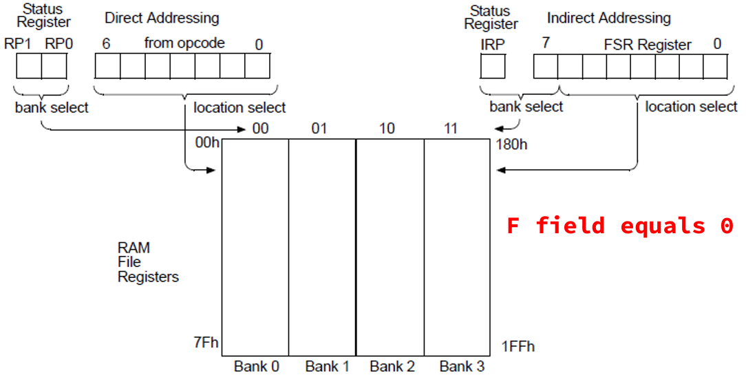
Based on Figure 5, Code 8 should write to RP if direct addressing, otherwise if indirect addressing IRP should be FSR. Code 8. Affective addressing for core module // Effective Address wire [ 8 : 0 ] EA; assign EA = ( `IRF == 0 ) ? { IRP , FSR [7:0] } : { RP , `IRF}; 2.4 Program Counter and Return Stack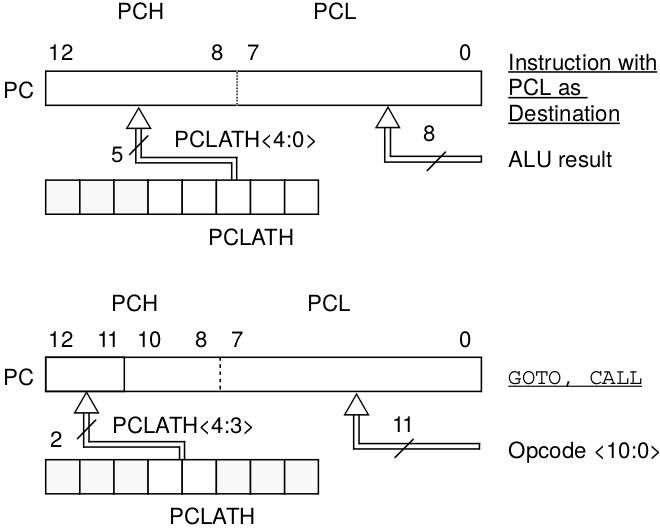 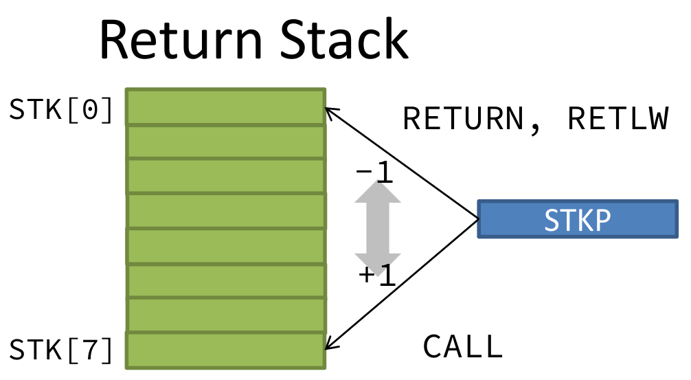
For Code 9 about program counter and return stack, the value of PC is based the left diagram of Figure 6. When operation call, then the stack is pushed, and when operation return, then the stack is popped. The value of STKP should be based on the right diagram of Figure 6. Code 9. Program counter and return stack // Program Counter & Return Stack reg [ 12:8 ] STK[0:7]; // Return Stack depth 8 reg [ 2:0] STKP; // Return stack pointer 4 bit reg STK_PU; // Stack Push enable reg STK_PO; // Stack Pop enable reg PC_W; // Write enable for CALL, GOTO // Program Counter always @( posedge CLK ) if( RST ) PC <= 0; else // RESET if( PC_W ) PC <= {PCLATH[4:3],IR[10:0] }; else // CALL, GOTO if( F_W && EA [6:0] == `A_PCL ) PC <= { PCLATH[4:3], WDATA[7:0] }; else // write PCL register if( STK_PO ) PC <= STK[ STKP-1 ]; else // RETURN, RETLW if( SLEEP || SLP_S ) PC <= PC ; else // SLEEP mode PC <= PC + 1; // Return Stack always @( posedge CLK ) begin if( RST ) STKP<= 0 ; else // for Empty if( STK_PU ) begin STK[ STKP ] <= PC ; STKP<= STKP+1; end else // for CALL if( STK_PO ) STKP<= STKP-1; // for RETxx end 2.5 Instruction Memory and Register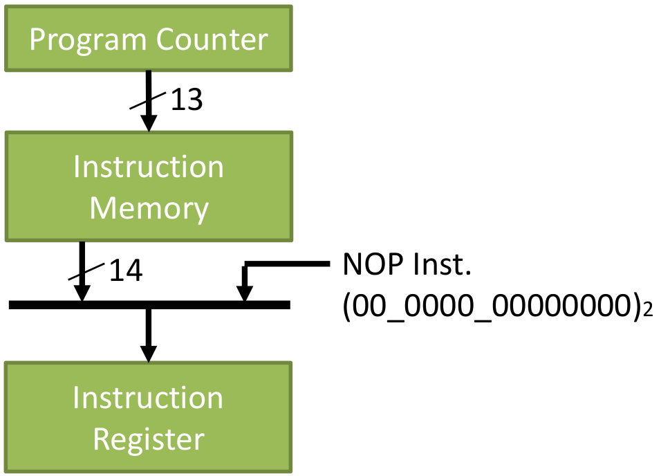 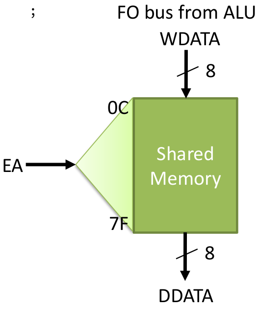
Code 10. Instruction memory and Register // Instruction Memory (8k word) reg [ 13 : 0 ] IMEM[ 0 : 8195 ]; initial begin $readmemh( PROG, IMEM ); end // Instruction Register always @( posedge CLK ) if( NOP_S || PC_W || STK_PO || RST ) IR <= 14'b00_0000_0000_0000 ; else // if CALL, RET, cond.SKIP IR <= IMEM[PC] ; // Instruction fetch 2.6 Decode and ControlTo write Code 11, the instruction table and instruction details on the datasheet [3] should be referred. Code 11 is written starting from first two bits of the instructions then the next 4 bits of the instructions. Refer again to the datasheet [3] of which status are affected. Unfortunately, sleep here is a repeat NOP. Code 11. Decode and control // Decode & Control always @( IR or ZO ) begin ALU_CB=IR[ 12 : 8 ]; F_W=0; W_W=0; Z_W=0; DC_W=0; C_W=0; nTO_S=0; nTO_C=0; nPD_S=0; nPD_C=0; STK_PU=0; STK_PO=0; NOP_S=0; PC_W=0; WDT_C=0; SLP_S=0; case( IR[ 13 : 12] ) 2'b00 : begin W_W = ~IR[7] && IR[11:8] != 4'b0000 ; F_W = IR[7]; //same with W_W = IR[7] && |IR[11:8] meaning bit 8 is 1 and bit 9-12 isn`t 0 case( IR[ 11 : 8 ] ) 4'b0000: case( IR[7] ) 1'b0: case( IR[ 6 : 0 ] ) 7'b000_1000 : begin NOP_S=1 ; STK_PO=1 ; end // RETURN // 7'b000_1001: ; // RETFIE 7'b110_0011 : begin nTO_S=1; nPD_S=1; WDT_C=1; SLP_S=1 ; NOP_S=1 ; end // SLEEP // 7'b110_0100: ; // CLRWDT default: ; // NOP endcase 1'b1: ; // MOVWF f endcase 4'b0001: begin Z_W=1 ; end // CLRW, CLRF 4'b0010: begin C_W=1 ; DC_W=1 ; Z_W=1 ; end // SUBWF 4'b0011: begin Z_W=1 ; end // DECF 4'b0100: begin Z_W=1 ; end // IORWF 4'b0101: begin Z_W=1 ; end // ANDWF 4'b0110: begin Z_W=1 ; end // XORWF 4'b0111: begin C_W=1 ; DC_W=1 ; Z_W=1 ; end // ADDWF 4'b1000: begin Z_W=1 ; end // MOVF 4'b1001: begin Z_W=1 ; end // COMF 4'b1010: begin Z_W=1 ; end // INCF 4'b1011: begin NOP_S= (ZO==1) ? 1 : 0 ; end // DECFSZ 4'b1100: begin C_W=1 ; end // RRF 4'b1101: begin C_W=1 ; end // RLF 4'b1110: ; // SWPF 4'b1111: begin NOP_S=ZO ; end // INCFSZ endcase //IR end 2'b01 : begin case( IR[ 11 : 10 ] ) 2'b00 : F_W = 1 ; // BCF f, b 2'b01 : F_W = 1 ; // BSF f, b 2'b10 : NOP_S=ZO ; // BTFSC f, b 2'b11 : NOP_S=~ZO ; // BTFSS f, b endcase end 2'b10 : begin PC_W = 1 ; NOP_S = 1 ; case( IR[ 11 ] ) 1'b0 : STK_PU = 1 ; // CALL 1'b1 : ; // GOTO endcase end 2'b11 : begin W_W= 1 ; casex( IR[ 11 : 8 ] ) 4'b00xx : begin ALU_CB=`IPSF ; end // MOVLW k //--> pass in ALU to W // 4'b01xx : begin ALU_CB=`IPSF ; STK_PO = 1 ; NOP_S = 1; end // RETLW k 4'b1000 : begin ALU_CB=`IOR ; Z_W = 1 ; end // IORLW k 4'b1001 : begin ALU_CB=`IAND ; Z_W = 1 ; end // ANDLW k 4'b1010 : begin ALU_CB=`IXOR ; Z_W = 1 ; end // XORLW k 4'b110x : begin ALU_CB=`ISUB ; C_W=1 ; DC_W=1 ; Z_W = 1 ; end // SUBLW k 4'b111x : begin ALU_CB=`IADD ; C_W=1 ; DC_W=1 ; Z_W = 1 ; end // ADDLW k endcase end endcase end // always @ ( IR or ZO ) 2.7 Special Register
Code 12 about special register is based on Figure 3 memory map for the written bits and Figure 8 about special register itself for its values. Code 12. Special register // Special Register // Write always @( posedge CLK or posedge RST ) begin if( RST ) begin C = 0 ; DC = 0 ; Z = 0 ; IRP = 0 ; RP = 2'b00 ; nTO = 1 ; // nTO=1 on Power-on nPD = 1 ; // nPD=1 on Power-on FSR = 0 ; PCLATH = 5'b00000 ; PORTA = 8'b0000_0000 ; TRISA = 8'b1111_1111 ; // All ports for input PORTB = 8'b0000_0000 ; TRISB = 8'b1111_1111 ; // Table page 18-20 // All ports for input end else begin // STATUS if( C_W ) C = CO ; if( DC_W ) DC = DCO ; if( Z_W ) Z = ZO ; if( nPD_S ) nPD = 1'b1; if( nPD_C ) nPD = 1'b0; if( nTO_S ) nTO = 1'b1; if( nTO_C ) nTO = 1'b0; // Register Write if( F_W ) //pic16_behaviour page 41 casex( EA ) //effective address // 9'b?0_000_0001: TMR0 = WDATA; // 01 101 Described TMR0 part //find in address table // 9'b?1_000_0001:`OPTION = WDATA; // 81 181 // 9'b??_000_0010: PCL = WDATA; // 02 82 102 182 Described PC part 9'b??_000_0011:`STATUS = WDATA; // 03 83 103 183 9'b??_000_0100: FSR = WDATA; // 04 84 104 184 9'b00_000_0101: PORTA = WDATA; // 05 9'b01_000_0101: TRISA = WDATA; // 85 9'b?0_000_0110: PORTB = WDATA; // 06 106 9'b?1_000_0110: TRISB = WDATA; // 86 186 // 9'b??_000_0111: ; // 07 // 9'b??_000_1000: ; // 08 EEDATA not implement // 9'b??_000_1001: ; // 09 EEADR not implement 9'b??_000_1010: PCLATH = WDATA[4:0]; // 0A 8A 10A 18A // 9'b??_000_1011:`INTCON = WDATA; // 0B 8B 10B 18B endcase end end Code 13. Data RAM // Data RAM (Write) always @( posedge CLK ) begin if( F_W && ( EA[6:0] >= 7'b001_1000 ) ) RAM[ EA[6:0] ] <= WDATA ; //12-127 PIC16 behaviour p.46 //light behaviour p.41 //Effective Address only 7bit not 9bit start from 12 //store RAM to WDATA end // Selecter for Special Register always @( IR or PC or EA or IRP or RP or nTO or nPD or Z or DC or C // STATUS or FSR or RA or TRISA or RB or TRISB or PCLATH ) casex( EA ) // 9'b?0_000_0001: SDATA = TMR0; // 9'b?1_000_0001: SDATA =`OPTION; 9'b??_000_0010: SDATA = PC[7:0] ; // PCL 9'b??_000_0011: SDATA =`STATUS ; // STATUS 9'b??_000_0100: SDATA = FSR ; // FSR 9'b00_000_0101: SDATA = PORTA ; // RA 9'b01_000_0101: SDATA = TRISA ; // TRISA 9'b?0_000_0110: SDATA = PORTB ; // RB 9'b?1_000_0110: SDATA = TRISB ; // TRISB 9'b??_000_1010: SDATA = {3'b000, PCLATH }; // PCLATH //because SDATA is 9 bit and PCLATH is only 6 bit, we need to add 3 bit before PCLATH // 9'b??_000_1011: SDATA =`INTCON; default: SDATA = 8'bxxxx_xxxx; endcase // Data RAM Read assign DDATA = RAM[EA[7:0]] ; 2.8 Data Path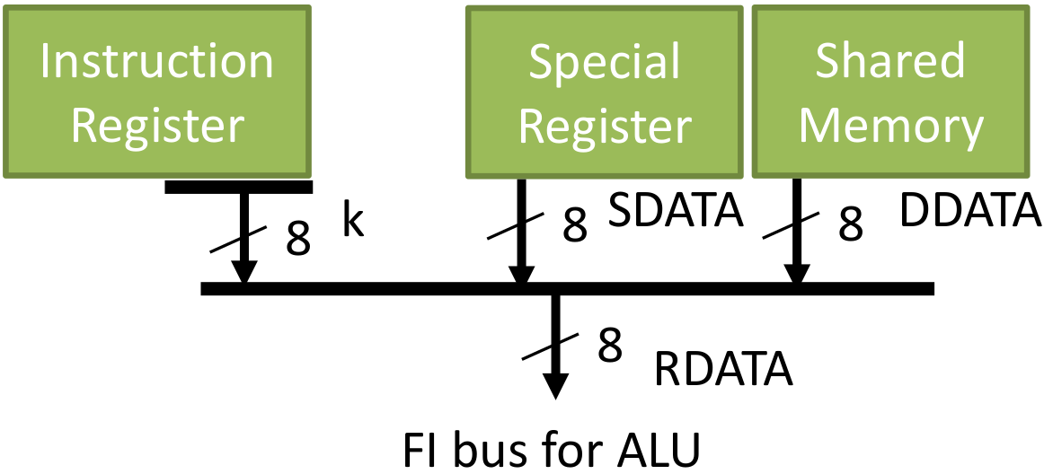
Code 14. Data selector for ALU // Data selector for ALU operand always @( IR or EA or DDATA or SDATA ) begin RDATA <= 8'bxxxx_xxxx ; if( &IR[13:12] ) RDATA <= `IRK ; else // casex( EA ) 9'b??_000_0010: RDATA <= SDATA ; // PCL 9'b??_000_0011: RDATA <= SDATA ; // STATUS 9'b??_000_0100: RDATA <= SDATA ; // FSR 9'b0?_000_0101: RDATA <= SDATA ; // PORTA, TRISA 9'b0?_000_0110: RDATA <= SDATA ; // PORTB, TRISB 9'b??_000_1010: RDATA <= SDATA ; // PCLATH default: RDATA <= RAM[EA[7:0]] ; // Shared memory endcase end 2.9 ALU Initiate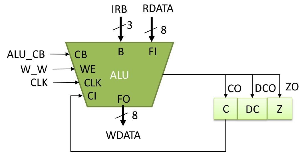
Code 15. ALU initiate code // Execute alu i_alu ( .CLK(CLK), .CB(ALU_CB), .WE(W_W), .B(`IRB), .FI(RDATA), .FO(WDATA), .CI(C), .CO(CO), .DC(DCO), .Z(ZO) ); 2.10 SleepBack on Code 11, sleep is a repeat NOP. Here on Figure 9, waking up from sleep is not implemented, sleep forever but can be reset. 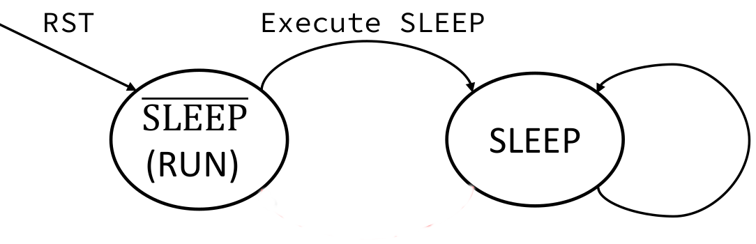
Code 16. Sleep implementation // Sleep mode always @( posedge CLK or posedge RST ) begin if(RST) SLEEP <= 0; else //0 mean run if(SLP_S) SLEEP <= 1; //1 mean execute the sleep mode end 2.11 Tristate Buffer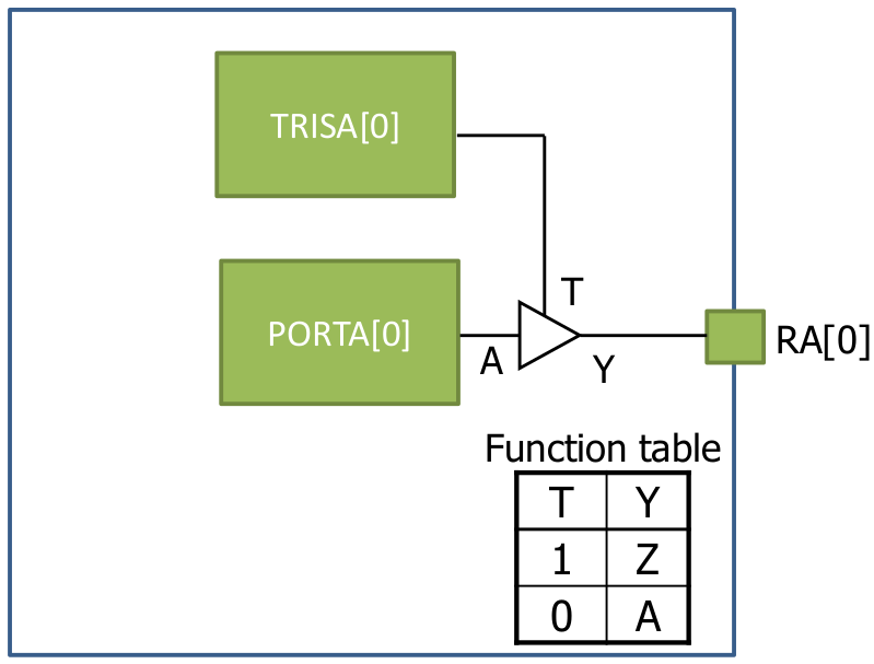
Code 17. Tristate buffer implementation // Tristate buffer for GPIO assign RA[0] = ( TRISA[0] ) ? 1'bZ : PORTA[0]; assign RA[1] = ( TRISA[1] ) ? 1'bZ : PORTA[1]; assign RA[2] = ( TRISA[2] ) ? 1'bZ : PORTA[2]; assign RA[3] = ( TRISA[3] ) ? 1'bZ : PORTA[3]; assign RA[4] = ( TRISA[4] ) ? 1'bZ : PORTA[4]; assign RA[5] = ( TRISA[5] ) ? 1'bZ : PORTA[5]; assign RA[6] = ( TRISA[6] ) ? 1'bZ : PORTA[6]; assign RA[7] = ( TRISA[7] ) ? 1'bZ : PORTA[7]; assign RB[0] = ( TRISB[0] ) ? 1'bZ : PORTB[0]; assign RB[1] = ( TRISB[1] ) ? 1'bZ : PORTB[1]; assign RB[2] = ( TRISB[2] ) ? 1'bZ : PORTB[2]; assign RB[3] = ( TRISB[3] ) ? 1'bZ : PORTB[3]; assign RB[4] = ( TRISB[4] ) ? 1'bZ : PORTB[4]; assign RB[5] = ( TRISB[5] ) ? 1'bZ : PORTB[5]; assign RB[6] = ( TRISB[6] ) ? 1'bZ : PORTB[6]; assign RB[7] = ( TRISB[7] ) ? 1'bZ : PORTB[7]; endmodule 3. Simulation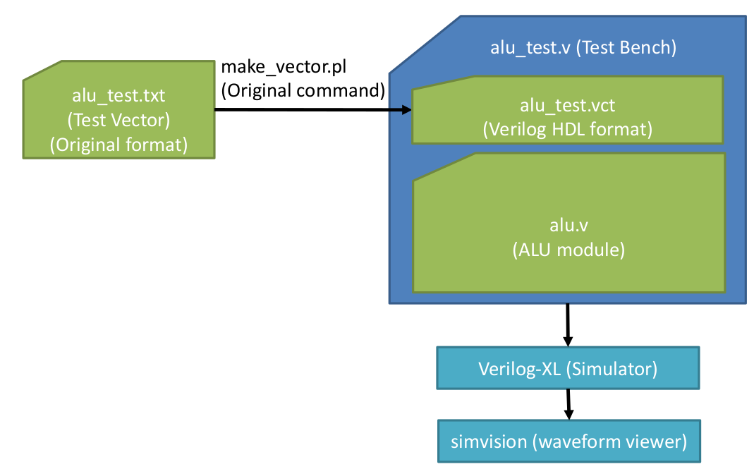
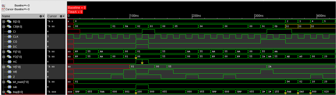
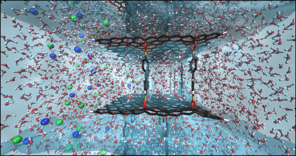
All the codes to conduct the simulation are available online [4]. For solely testing the ALU, follow Figure 13 which are about generating the clock, and testing operations starting from PASSF, subtraction, until bit test. Figure 13 compiles the test sequence from text format into verilog HDL format using make_vector.pl binary. Then these files including Code 1-6 is compiled using verilog binary. The waves can be examined using simvision which can be shown on Figure 14. All the wave values are shown in hexadecimals. CB shows the executed operation. It is seen the W register becomes 1 when performed an increment operation, and reduced to 0 when subtract operation was performed, note that HC and CO has started to become affected. After that is logical operation where the result can be seen on FO as well. In the ends of this simulation is where the bit manipulation operations are performed where the B and bitmask variables are affected. 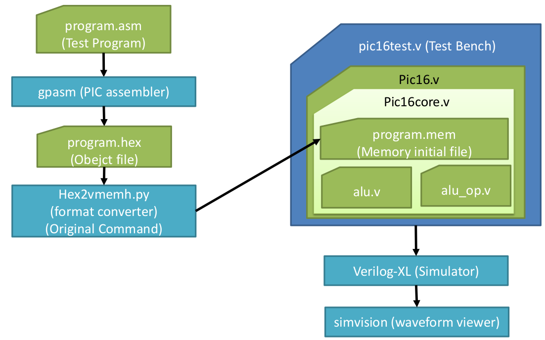
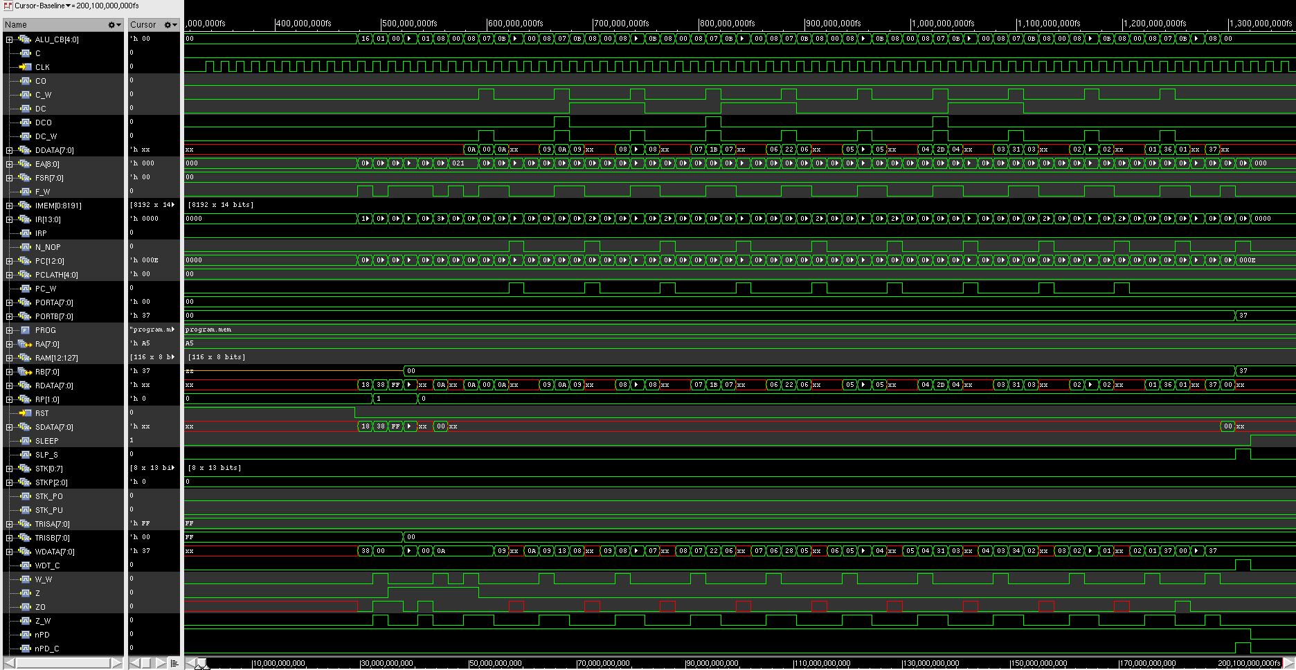
Figure 15 shows the diagram of testing the PIC16 core. The program.asm shows that only 10 operations are tested [4]. Next it have to be converted into an assembly file using gpasm which then the format have to be converted. After that the PIC16 core whole files [4] can be compiled using verilog and the waves can be seen using simvision on Figure 16. The first part of the test should bitset the RP, clear W, set TRISB to 00h, bitclear RP. The next operations are to do ten times addition of ten. DData, RData, and WData should look consistent. First the value should be 0A which is hexadecimal of 10, then it should increase to 1B and everytime added by 10. Note that the decrements are also shown from 0A until 01. In the end the result is 37 and will be transferred to PORTB. The last operation is sleep. Note that the design on this report does not implement everything from the original as shown on Table 1. Table 1. Original PIC16 versus this report’s design
4. ImplementationThe verilog HDL codes can be implemented in FPGA. On this report Nexys4 DDR board is used on Figure 17 and Vivado software is used to synthesize the code. The LED should show 110111(2) which is 37 that is the result of the addition. 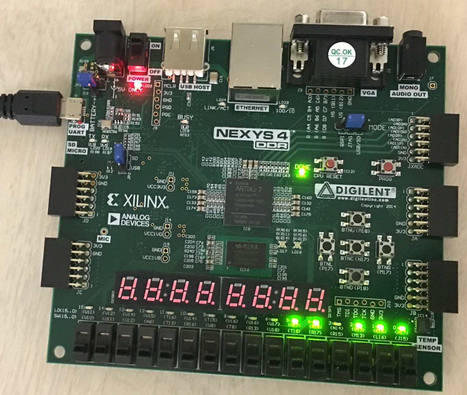
5. Reference
0 Comments
NoteThis is one of my Doctoral assignment from Current Science and Technology in Japan Course which has never been published anywhere and I, as the author and copyright holder, license this assignment customized CC-BY-SA where anyone can share, copy, republish, and sell on condition to state my name as the author and notify that the original and open version available here. Pipelining for microprocessorA microprocessor is an electronic component that is used by a computer to do its work. It is a central processing unit (CPU) on a single integrated circuit (IC) chip containing millions of very small components including transistors, resistors, and diodes that work together [1]. The traditional microprocessor is too simple, but it is good to be explained in the class. The traditional one have five instructions which in order are fetch, decode, execute, memory, and write. In Figure 1 is seen that the program counter accesses the instruction memory, then the register fetch the instruction, next the instruction is decoded by the decoder, later it is sent to the arithmetic logic unit (ALU) and execute the instruction, finally the result is stored in the data memory and written into the register [2]. 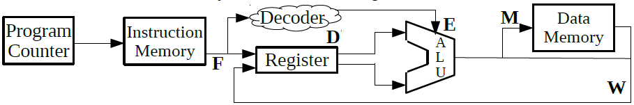
Pipelining is a technique to speed up the processing. Without pipelining the processor will have to wait until the whole 5 steps finishes before it can execute a new one, in other words serial processing. However pipelining allows the processor to start processing the next instruction without waiting until the previous instruction processing is finished, in other words parallel processing. Figure 2 showed the simplest illustration, but the technique have grown vast, for examples there are parallel operation, superscalar, super pipelining, and very long instruction word (VLIW). There are also data dependency problems such as flow, control, anti, intput, and output that prevents performance improvement. There are some techniques such as data forwarding, and dynamic code scheduling. [3] 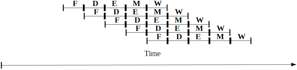
GPGPU and CUDAGPGPU was originally graphic processing unit (GPU) which is to process graphics, whether they are 2D (dimension) or 3D, still picture or moving picture (movie), and there are also animations and games, not to forget that the monitor is refreshing around sixty times a second. Just to process a single graphic took a lot of math or algorithms which is very heavy for the CPU which is why back then engineers created GPU solely to handle graphics. Today an innovation was made that GPU can be used for general purpose, and now comes the term general purpose graphic processing unit (GPGPU). [4] Respectively the current intel i7 processor have 4 processing units (cores) while a GPGPU can have hundreds of cores, the current Geforce GTX 1080 Ti have 3584 cores. Figure 3 showed an illustration of CPU versus GPU. The essence of GPGPU is parallel processing (most people agree back when it was a GPU, it was used to parallel process the pixels in graphics). Nvidia created CUDA which is a parallel computing platform and programming model that allows to utilize their GPUs into GPGPUs. The simplest example is performing a loop program for example a hundred loops. In a CPU the loops is processed in serial order from one to a hundred, while in GPGPU the hundred loops are processed in an instant (depending on the number of cores). The processing speed greatly increases, I have example codes in C, C++, python, octave, and R which compares running in CPU and GPGPU using CUDA and OpenACC [5]. However GPGPU can only run non-specialized processes, which why CPU is still needed. The theory is long, but simply the process is first defined in the CPU, then the CPU divides the process to the cores in GPGPU, lastly the GPGPU returns the result to the CPU. 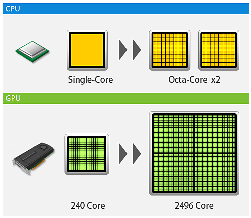
Open MP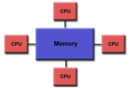
Openmp stands for open multiple-processing, it is an application program interface (API) that provided parallelism in shared memory through the implementation of multi-threading. Since it is in shared memory, openmp is only utilizable on multi-core CPUs, where shared memory is a certain space on the memory to be shared by other cores on the CPU. The other keyword is thread, where it is the smallest unit of a process which can be scheduled. A process can be single thread or multi-thread. Openmp allows the threads to run in parallel speeding the process and optimizing the use of resources. The core elements of OpenMP are the constructs for thread creation, workload distribution (work sharing), data-environment management, thread synchronization, user-level runtime routines and environment variables. Openmp supports C, C++, and fortran. Back on my coding in openacc [5], the pragma directive “acc” can be changed to “omp” to use openmp in the code. [6] 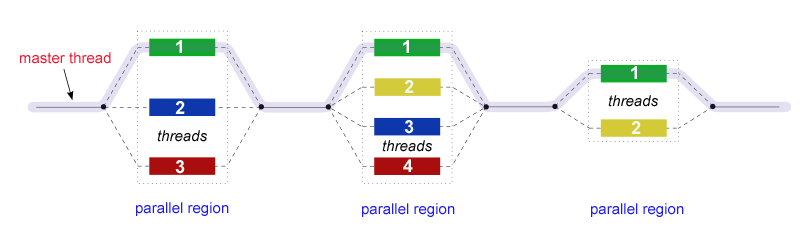
Open CLOpencl stands for open computing language. Although mostly today people elevate it for its parallelism, opencl is not just parallelism but an open standard computing language which supports heterogeneous or many kinds of systems such as CPUs, GPUs, digital signal processors (DSPs), mobiles, and even FPGAs. There are many more devices that it supports, unlike CUDA which only supports Nvidia devices. Although CUDA is great for personal projects because it has more libraries and better programming interface, but if the product is to be commercialized, then opencl is preferable because it supports many devices. Also if purely want to make the code as open as possible, opencl is best because of its compatibility. The code that was made can be portable to all sort of devices. The coding of opencl is based on C99, but today it also supports C++11. The concept parallelism is almost the same as CUDA, openmp, and openacc. [7] Reference
This is one of my Doctoral assignment from Current Science and Technology in Japan Course which has never been published anywhere and I, as the author and copyright holder, license this assignment customized CC-BY-SA where anyone can share, copy, republish, and sell on condition to state my name as the author and notify that the original and open version available here. Graphene is a single layer of carbon atoms arranged in interconnected hexagonal lattice. It attracts the attention of lots of researchers, some calls it a wonder material, a miracle substance, or a substance that made people confused that it is substance that is only found in a comic book, all due to its amazing properties. It is one atom thick, conducts electricity better than silver, it conducts heat better than diamond, it is stronger than steel, it is lighter than feather, it is transparent, and it is bendable. Examples application possibilities are can replace a silicon transistors to graphene transistors in computers which can raise the frequency ten times from 100 to 1000 gigahertz, it can be used to make an unbreakable device screen, and as a better material for water disalination. Graphene was founded in 2004 by Andre Geim and Konstantin Novoselov from University of Manchester. They used a simple method using scotch tape to peel off graphite (the lead of a pencil) or stacks of graphene sheets into a single graphene sheet. Although graphene have huge amazing properties, it is still a future material because it is very difficult to produce and very expensive for mass production. [1] [2] [3] Since graphene is very difficult and expensive to produce, researchers divides their attention to the graphene’s derivatives. Though its derivatives have less amazing properties, the properties can be tuned by going through certain processes. One of its derivatives is graphene oxide is a single-atomic layered material, made by the powerful oxidation of graphite. It can be said as an oxidized form of graphene laced with oxigen containing groups. It is considered easy to process since it is dispersible in water (and other solvents), and it can even be used to make graphene. It is commonly sold in powder form, dispersed, or as a coating on substrates. There are four basic methods of synthesizing graphene oxide which are Staudenmaier, Hofmann, Brodie and Hummers. [4] Reference
Mirrors
NoteThis is one of my Doctoral assignment from Current Science and Technology in Japan Course which has never been published anywhere and I, as the author and copyright holder, license this assignment customized CC-BY-SA where anyone can share, copy, republish, and sell on condition to state my name as the author and notify that the original and open version available here. Material Exploration and DiscoveryMaterials have been one of the based of technologies for millennia. Airplanes, accessories, apparels, buildings, cars, computers, televisions, weapons, almost every object we know is made up of materials. The field of material engineering, science, and those related became very famous and important to advance technology. Before the 17th century is an age of exploration. There were many adventures/explorers back then who traveled the lands, and sailed the seas, finding new territories. They discovered stones, irons, bronzes, silvers, golds, diamonds, aluminiums, minerals, and many other resources to be used in people’s live. Starting on the 17th century is an age of discovery where many alchemist, philosophers, and scientist research and perform experiments which birth for examples the theory of atoms by John Dalton, polymers and molecules by Hermann Staudinger, electricity by Thomas Edison, engine by Edward Butler, and more material properties and process were found on this age. It is mostly due to the advance in engineering and other related disciplines that invented tools such as microscope, pyrometer, and x-ray. These led to many inventions such as electronic devices, vehicles and many other tools and machines that shaped this modern era. Today a new age is approaching. The field of materials science and engineering is shifting into a more systems based approach to materials innovation and toward materials design in which researchers can predict new materials they would like to have rather than having to discover them. [1] Material DesignThe coming age is the age of design. With the discovery of many raw materials, processes, and theories, researcher may now utilize these accumulated data to design new materials, depending on the demands such as conductivity, strength, elasticity, resistance, texture, and many other features. Some examples of new materials today are cheap carbon fibers, nano crystals for solar harvesting and quantum computing, semi conductor materials, and our own kumadai magnesium alloy. Designing can be through calculations, computations, and simulations, which can greatly reduce the cost since there is less need for experiments and trials, in other words less wasting raw materials and reducing the risks of fail experiments which is uncertain of how much can be loss. However with the vast amount of data there is a limit to how fast a human can perform. Therefore researchers turn to computers that can perform millions of instructions per seconds, in other words by utilizing computers researchers can obtain much faster results which saves time. [2] My Suggestion from Computer ScienceMy role in the field of computer science and electrical engineering is to develop applications and computer devices to assist researchers in material science and engineering. The very basic that can be done is to increase the computer’s hardware performance where the basic units are computer processing unit (CPU), random access memory (RAM), hard drive (HD) or disk storage, and graphic processing unit. Hardware is already the major attention of many big companies. For hardware also there are many collaboration from many disciplines including material science and engineering. For example the CPU’s transistors are made of silicons, imagine if graphene is made available to be implemented in the transistors, it can make computer 10x faster. Another example is the heat sink which looks simple but vital, without the help of material experts, computers will be facing overheat problems by now. Other than basic hardware, there are accelerators such as general purpose graphic processing unit (GPGPU) and field programmable array (FPGA). These two supports parallel processing, and was tested to able to speed up a program up to 100x. Recently, material computations not only uses regression analysis alike, but also uses machine learning such as neural network. Although I’m not sure in the field of material science and engineering itself, but in computer science we are used to train big data where on a regular computer may usually take days, which is why we incorporate accelerators such as these (GGPU and FPGA). If it is similar in material computations, then accelerators can be utilized. Although utilizing accelerators requires to reconfigure the material computation program or simulator, sometimes reprogramming is required, these can be done by a programmer, Nvidia provides cuda libraries [3]. Aside from accelerators, today portable computer devices are trending such as micro-controller Arduino, single board computers such as Raspberry Pi [4], and some sensor boards. They be used on the field like in caves, forest, and mines for example because they are hand carry device, very small (the size of a hand), and low energy consumption. While usually is not a good idea to carry computers to the field, it is no problem in carry these devices and they can perform almost as good as a computer. Lastly other than hardware are software and network. There many software available to perform analysis, even there are specific simulators for material experts. However most of the software known and used today are for personal use, while today the work environment in computers are slowly integrating to the cloud, another way of saying is that work environment is no longer personal but connected, collaborated with other users on the computer network. The integrated computational materials engineering (ICME) system which have a web interface and database is quite close with the cloud environment [2]. There has not exist an online material simulator, but it is possible make. On a certain a website in cavasmol there are people who had created some sort of web molecule simulator [5]. Although basic communications can be achieved through emails, messengers, and social networking services (SNSs), a collaboration is yet to be available for online collaborations of material computation For example in my field of computer science there is a platform called github to collaborate on codings [6]. This is something we can assist and collaborate in the future. Reference
My Description and Opinion
How to StartYou do not need to know about complicated technical knowledge. You do not need to learn about decentralized finance (DeFi) to start eventhough it is best to be integrated in the future. To start, you only need to:
My video above only took 2 minutes:
Mobile Complete TutorialIn contrast to the desktop short getting started guide, if you access the dapp using a mobile device, you will get a much more detailed tutorial complete with animation. If you want to see this tutorial on desktop or again on mobile go to menu > settings > tutorial. Yeah, some of us are too lazy to try Upland or watch my video, so I rewrote the tutorial text fo you people here:
What New Players Today May Confuse About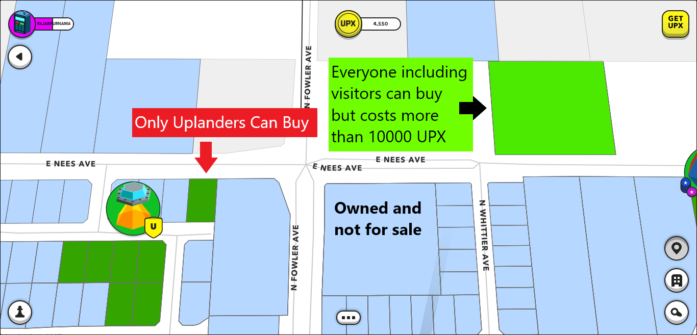
Mirrors
List of Decentralized Exchanges that Emerged in Early 2021 Outside of Ethereum with Affordable Fees8/3/2021 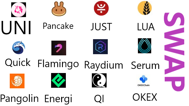
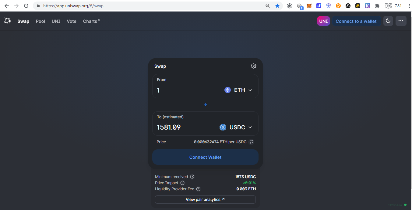
Early Decentralized Exchange on EthereumThanks to decentralized exchanges, we can enjoy convenient trading without custody and know your customer (KYC). With Uniswap, trading becomes much more simpler with just the press of the button. Unlike centralized exchanges (CEX) where we need to:
after:
Decentralized Exchanges Outside of Ethereum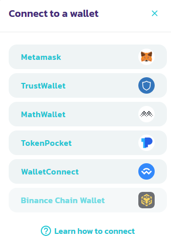
Binance Smart ChainThe following DEXs are on Binance Smart Chain ecosystem with all transactions paid in BNB. Note that it is different from Binance Chain ecosystem where the address starts in bnb..., this ecosystem uses the same address as Ethereum. Therefore, you can use Metamask by just switching networks: 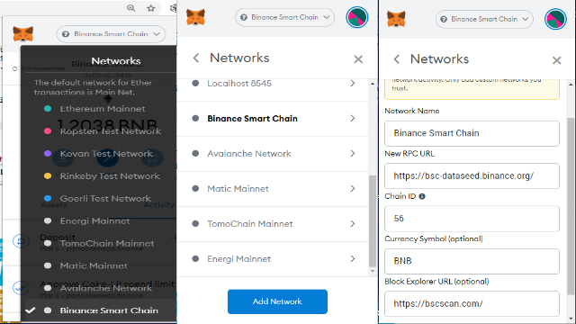
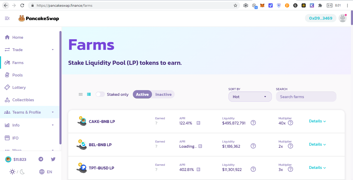
Disclaimer: do not trust even me easily, always check their official website for example https://academy.binance.com/en/articles/connecting-metamask-to-binance-smart-chain because you may get your fund stolen if you use a malicious RPC (please correct me if I am wrong). Still, I prefer to use the Binance Chain Extension as it provides cross chain transactions between Binance Chain (bnb....) and Binance Smart Chain (0x....). Pancake Swap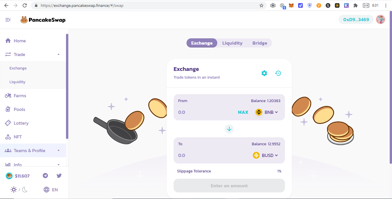
Other DEXsThe following DEXs originally just Ethereum DEXs but are integrating Binance Smart Chain into them: Binance Chain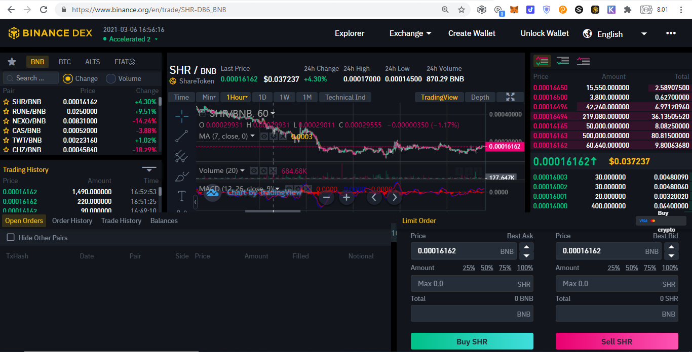
Tron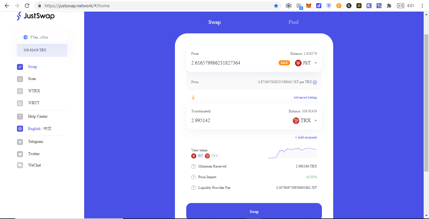
There are other Tron DEXs other than Just Swap but they are still using traditional order book: Tomo Chain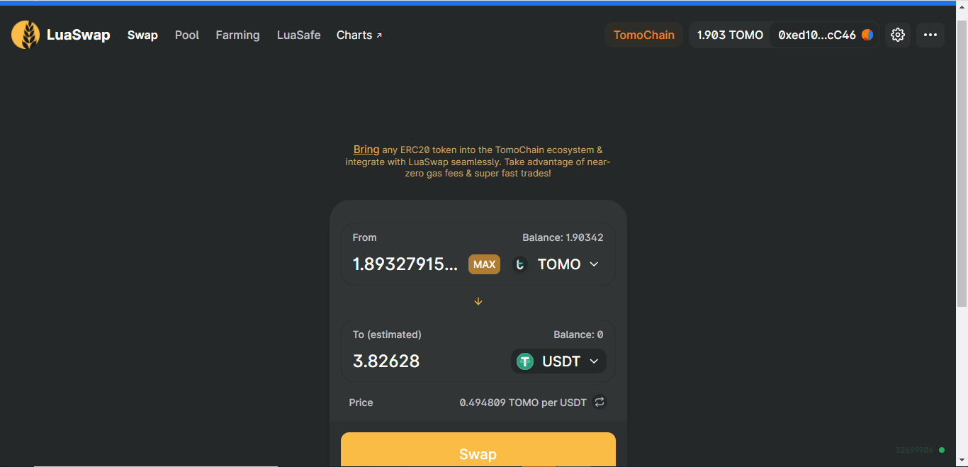
Matic/Polygon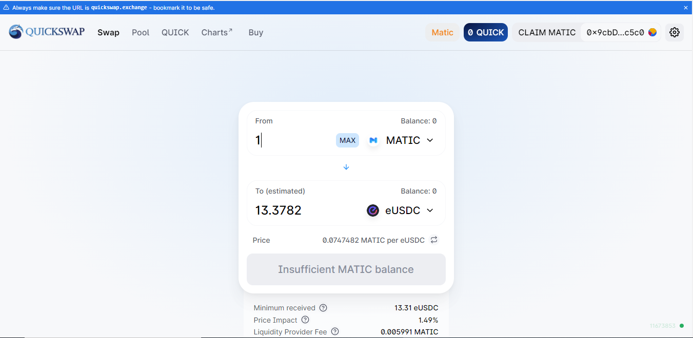
Neo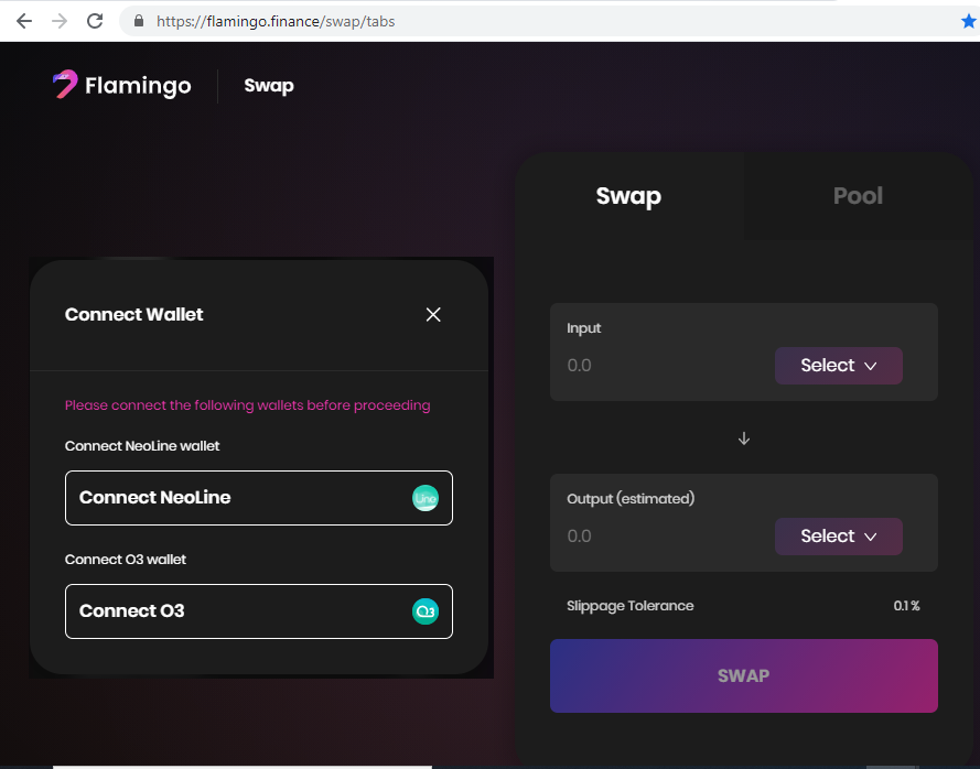
There are other DEXs which uses traditional orderbook: Zilliqa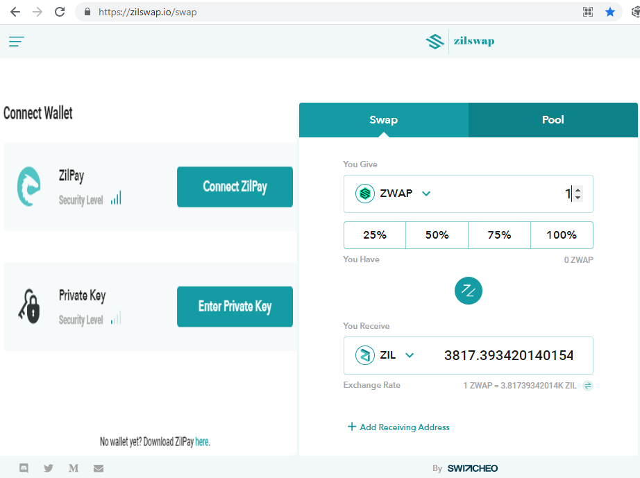
Solana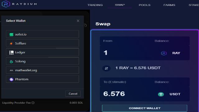
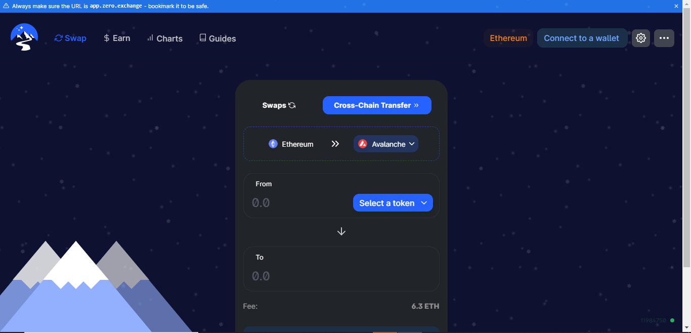
Avalanche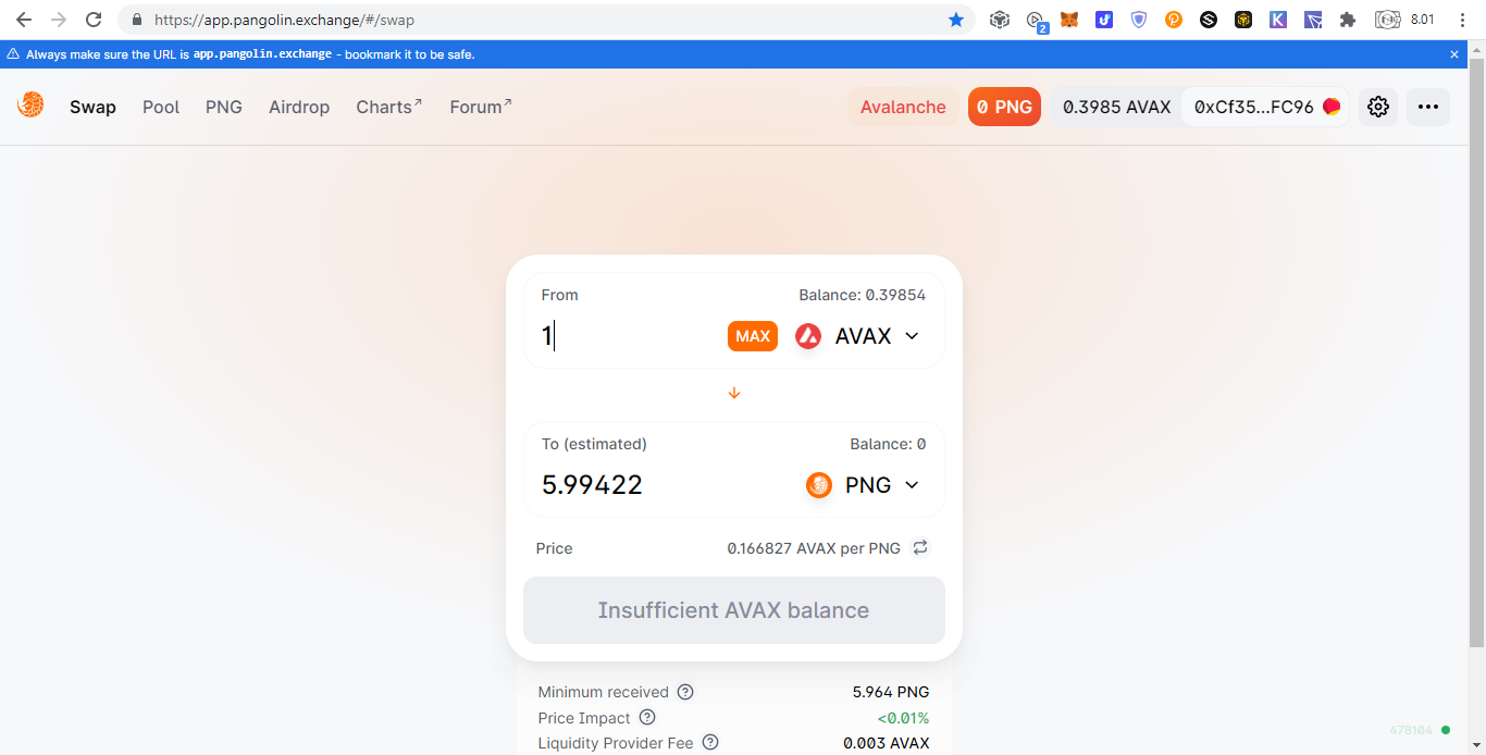
Energi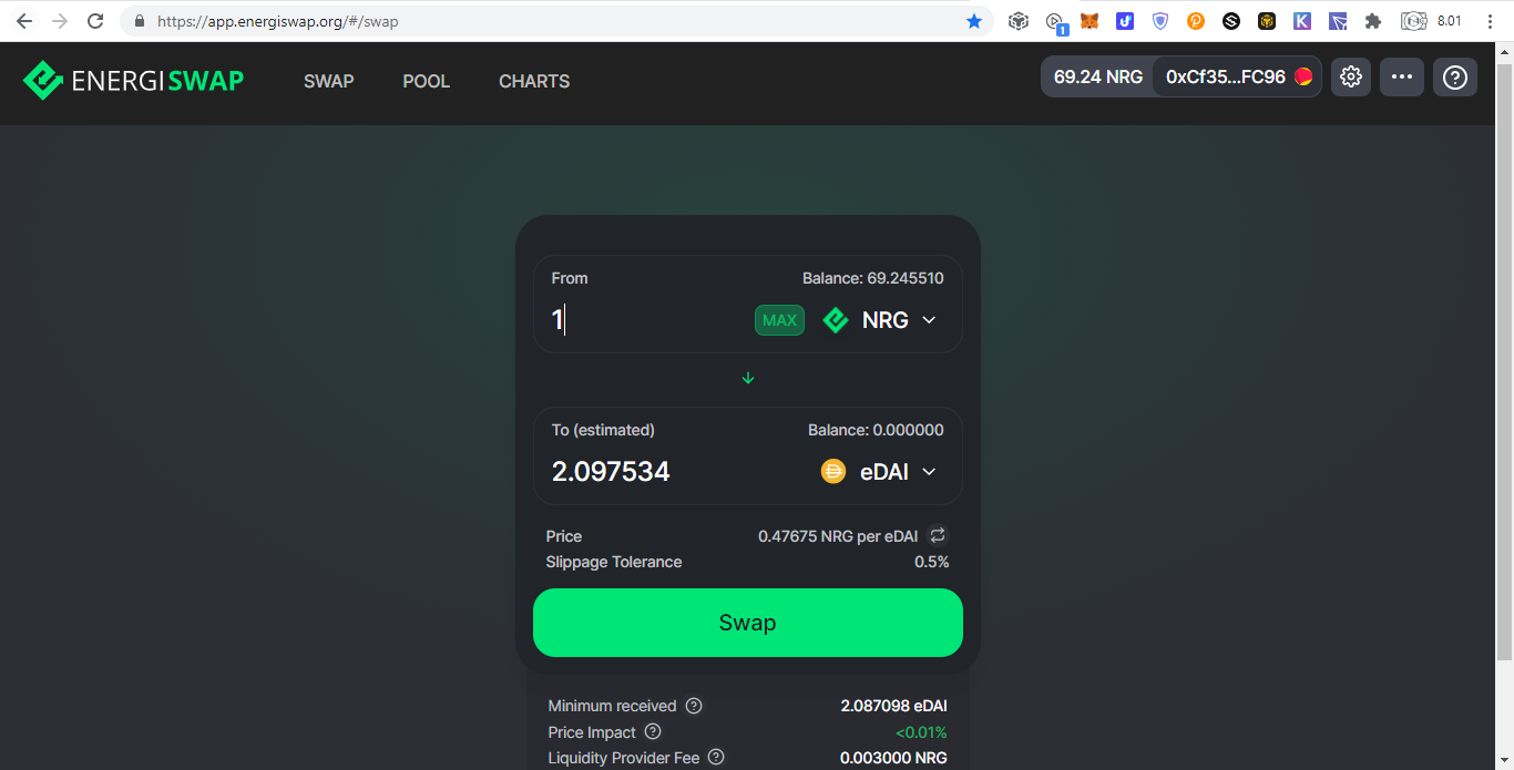
QTUM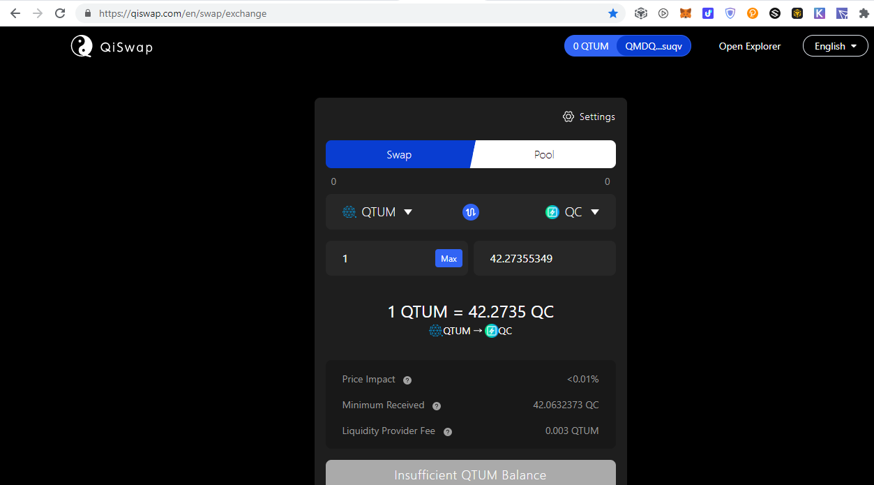
OKEX Chain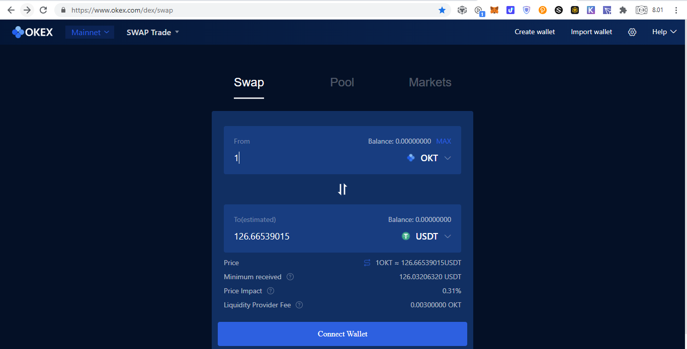
Cosmos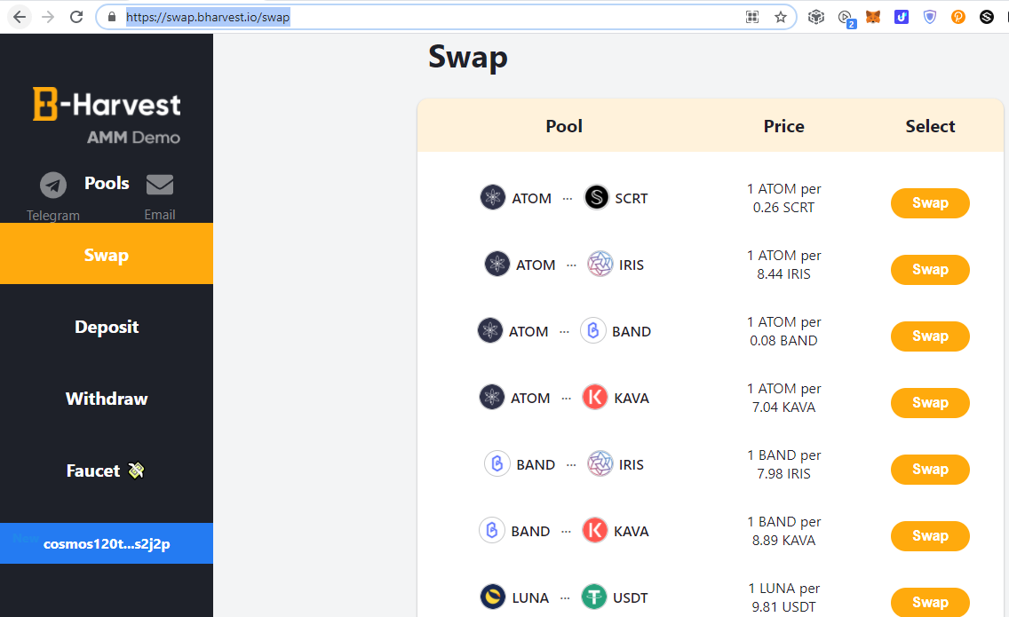
Sif Chain
Others Only Order Book
Finally, looking forward to Polkadot and other cross chain products. Leave a comment if you know anymore to complete this list.Content CreationBlogs
Videos
Images
Personal Monetization
Common TasksBrowsing
Cointiply
ReferralsCurrently the quantity is too much to handle when the value I earned is not much. So I may report this on a separate article. January 2021 Income ≈ $102.1443Grade: CPersonal CommentsThough the dollar amount is one hundred but compared to previous months, I earned less coins. There were straight 10 days that I did not blog. As a Torum ambassador, I should have write an article at least once a week but even that I cannot uphold. The reason was because the deadline of a project that I joined in the end of January. I was scouted many times but I never gave a proper answer but finally my friends and family were approached and I had no choice but to say yes because they told me to probably because they felt bothered seeing me unemployed and wanted me to physically socialize with other people more. I do not even know whether I will get paid or not. It is not just me but my friends and families said straight to my face that I get used alot by people and one of the solution is to get employed and learn different kind of people personalities and how to face them. Well since we have not met for years, they remembered of when I was in the past during my college times. It was half a year after I graduated that I was able to continue my studies abroad and escape my fate of being a tool. There I introspect myself and change myself. I no longer prioritize other people's dreams. My dreams comes first. I though being self sacrificing is noble but I learned the hard way that only in few circumstances like sacrificing your life to save others is worth it. Other than that, it is just stupid. Is it noble, self sacrificing your time, your future, and your happiness for the sake of other people's happiness? That is not self sacrifice but a fool being used as a tool. Yes, there are good people worthy to be called friends who shares their success with you and it is worth working hard not for them but alongside them. However, there are people who just asked for your help, never cared about you except for your contribution, and never contact you except when they need help. I believe with the current system now, most people are working to make other people rich. Once again, it is okay if they are good people who shares their success with you but what about they are people who takes most of the profit of your hard work? So, different from the past where I got used many times, I will prioritize my own missions first:
Gem hunting? Do you know that last few months, I won more than 100 months worth of average salary in my country? Sure that I did gamble, but it is a gamble with study and hard work. I explored countless cryptocurrencies, studied their fundamentals, checked the news and other people's sentiment, sorting profiles, medias, and portfolios, even used simple technical analysis, crazily starting to learn psychic as well, and finally made my decision. If I followed the herd and chose a busy employment, would I have achieved such a win? Ofcourse not, for example very unfortunately that the largest bull market started when I was recruited for the current project that I even missed the news of Elon Musk in Bitcoin and Dogecoin because those first days I was very busy right away. Before I was busy, I already put many crypto projects on my watch list and planned to invest, but this project suddenly came, suddenly became busy, and made me forget about my watch list. Finally after times got a bit relaxing again, I cried in my heart seeing all, I repeat all my watchlist went to the moon. It was too much for a coincidence for me, that I have been researching for a long time only to miss the bull market. Still, the people in the project now are good people where except for deadlines, I was allowed to work whenever and where ever I want so after the first busy days I was back to my missions above and busy again because of deadline in past 10 days. Yes, I do not know whether I get paid or not but chances are high if not me getting paid directly, my parents are the ones who will be paid since the agenda is me replacing them. At the very least, I have a chance to push my agenda to them which is introducing them to crypto and who knows maybe I can recruit them instead when in the future I start a crypto project. Appendix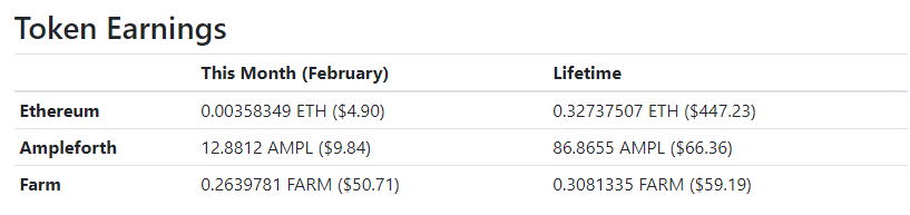

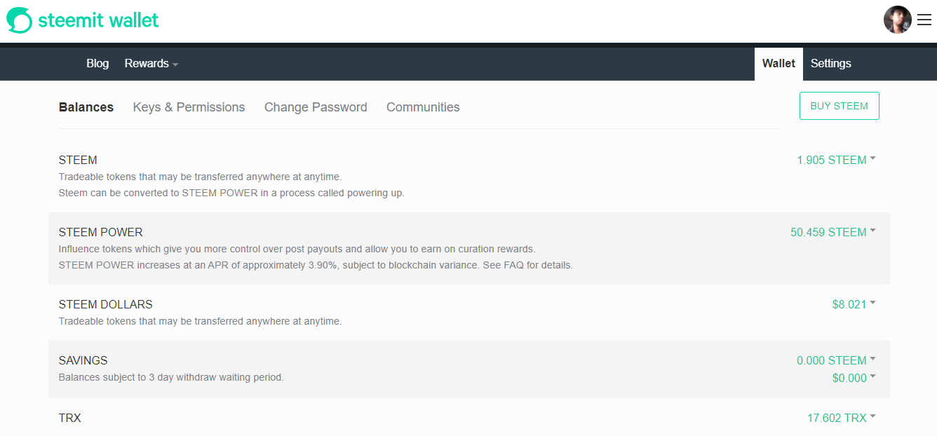
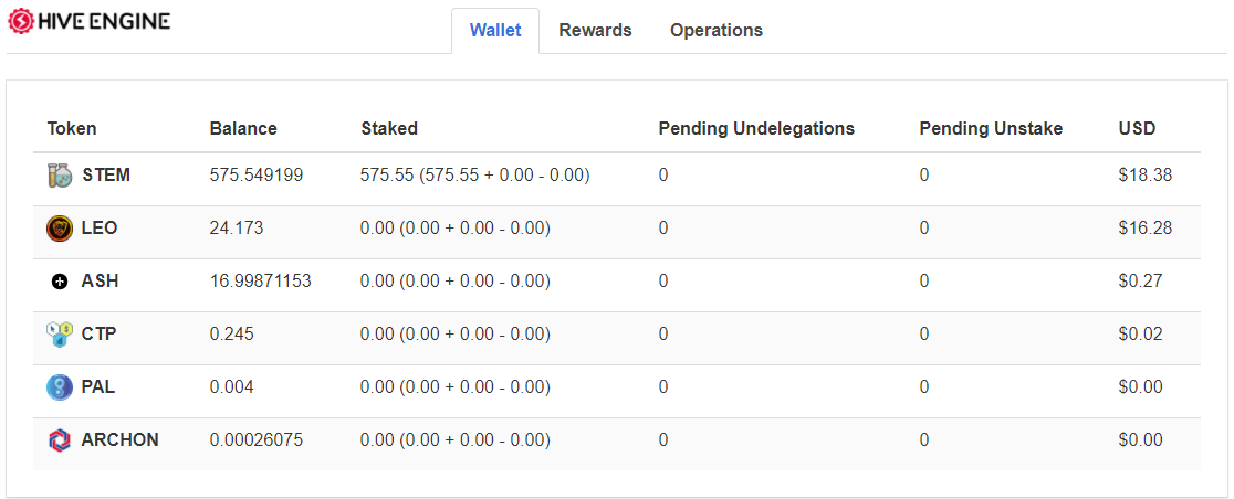
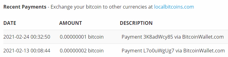
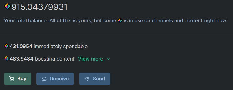
DonationPersonally, I enjoyed being a full time independent content creator very much and I once again thank the platforms, investors, donators, and viewers for making my venture possible through donations, tippings, and upvotes. If you enjoy and/or want to further support my work you may choose more form of donation:

|
Archives
August 2022
Categories
All
source code
old source code Get any amount of 0FP0EXP tokens to stop automatic JavaScript Mining or get 10 0FP0EXP tokens to remove this completely. get 30 0FP0EXP Token to remove this paypal donation. get 20 0FP0EXP Token to remove my personal ADS. Get 50 0FP0EXP Token to remove my NFTS advertisements! |
 RSS Feed

