My Report about PIC16F84A Microcontroller Implementation on Verilog Hardware Description Language23/3/2021 NoteThis is one of my Doctoral assignment from Advanced Computer Architecture II Course which has never been published anywhere and I, as the author and copyright holder, license this assignment customized CC-BY-SA where anyone can share, copy, republish, and sell on condition to state my name as the author and notify that the original and open version available here. 1. IntroductionPeripheral interface controller (PIC) is a family of microcontrollers made by Microchip Technology. A microcontroller is a one chip computer that include microprocessors, memories, and peripherals. PIC devices are popular with both industrial developers and hobbyists due to their low cost, wide availability, large user base, extensive collection of application notes, availability of low cost or free development tools, serial programming, and re-programmable Flash-memory capability. They can be programmed to be timers, to control a production line, to control light and sound intensity by involving few sensors, and to perform other kind of tasks. The PIC microcontroller have five basic instruction cycle which are fetch, decode, execute, memory, and write (FDEMW) . [1] 2. Verilog HDL Design
On the verilog hardware description language (HDL) design is based on Figure 1. This sections starts by constructing the arithmetic logic unit (ALU), bitmask, and W register. Then continue to design the program counter and return stack which its values to be sent to the instruction register where there is also decode and control behavior. Next is the design of special register, although the effective addressing is discussed in early part. After that the built module have to be connected to the firstly created ALU, bitmask, and W register. Lastly implement sleep and tristate buffer. 2.1 Arithmetic Logic Unit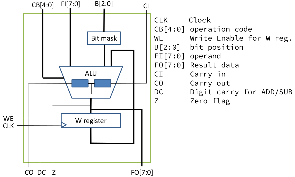
Code 1. Input and output of ALU module alu ( CLK, CB, WE, B, FI, FO, CI, CO, DC, Z ); input CLK;// Clock input [4:0] CB; // operation code input WE; // Write enable for W register input [2:0] B; // bit position input [7:0] FI; // operand input CI; // Carry in output [7:0] FO; // dest bus output CO; // Carry out output DC; // Half carry output Z; // Zero reg HC; // half carry reg [7:0] W; reg [8:0] tmp; reg [7:0] bit_mask; wire sub; assign sub = ( CB == `ISUB ); Code 2. Bitmask always @( B ) case( B ) 3'b000: bit_mask = 8'b0000_0001; 3'b001: bit_mask = 8'b0000_0010; 3'b010: bit_mask = 8'b0000_0100; 3'b011: bit_mask = 8'b0000_1000; 3'b100: bit_mask = 8'b0001_0000; 3'b101: bit_mask = 8'b0010_0000; 3'b110: bit_mask = 8'b0100_0000; 3'b111: bit_mask = 8'b1000_0000; default: bit_mask = 8'bxxxx_xxxx; endcase 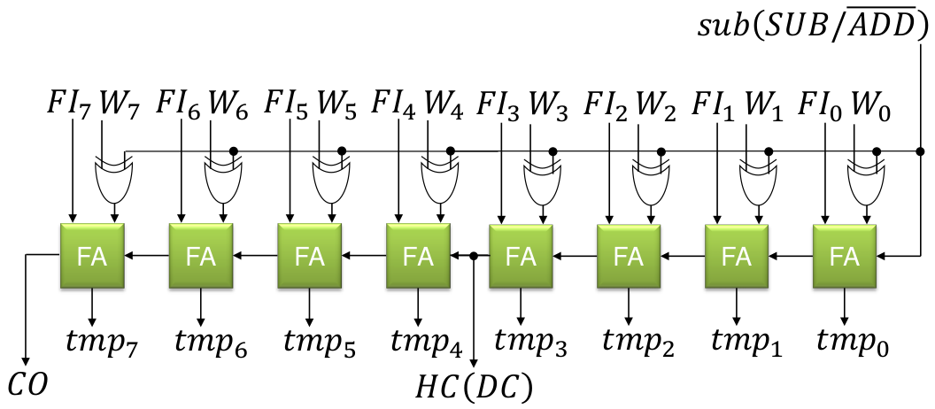
Code 3. Up to add and sub always @( CB or FI or W or HC or CI or bit_mask or sub ) begin HC = 1'b0; casex( CB ) ` IPSW: tmp = { 1'b0, W }; // Pass W register value `ICLR: tmp = 9'b0_0000_0000; // Clear `IADD, `ISUB: begin { HC, tmp[3:0] }= {1'b0,FI[3:0]} + {1'b0, sub? ~W[3:0]:W[3:0]} + sub; tmp[8:4] = {1'b0,FI[7:4]} + {1'b0, sub? ~W[7:4]:W[7:4]} + HC; end The verilog design of the ALU is based on the diagram on Figure 2. The input, output, and process looks clear which was implemented on Code 1, however the detail operation within the bitmask, ALU, and w register should be examined on Code 2, Code 3, and Code 4. The ALU operates between the value on the W register and the current input FI. For addition and subtraction, Code 3 should follow the diagram on Figure 3, while for other operations are not as complicated which is on Code 4. After that, the output can be written on Code 5. The operation definitions are available on Code 6 which the bit opcode from 2nd to 6th from left to right is used. Code 4. Other Operations `IDEC1, `IDEC2: tmp = { 1'b0, FI } - 1 ; // Decrement, Decrement and skip if 0 `IOR : tmp = { 1'b0, FI } | { 1'b0, W } ; // Logical OR `IAND: tmp = { 1'b0, FI } & { 1'b0, W } ; // Logical AND `IXOR: tmp = { 1'b0, FI } ^ { 1'b0, W } ; // Logical Exclusive OR `IPSF: tmp = { 1'b0, FI } ; // Pass FI `INTF: tmp = { 1'b0, ~FI } ; // Complement FI `IINC1, `IINC2: tmp = { 1'b0, FI } + 1 ; // Increment, Increment and skip if 0 `IRRF: tmp = {FI[0], CI, FI[7:1]} ; // Rotate Right through Carry `IRLF: tmp = {FI, CI} ; // Rotate Left through Carry `ISWP: tmp = {1'b0, FI[3:0], FI[7:4]}; // nibble swap `IBCF: tmp = {1'b0, FI} & {1'b0,~bit_mask} ; // bit clear `IBSF: tmp = {1'b0, FI} | {1'b0, bit_mask} ; // bit set `IBTF: tmp = {1'b0, FI} & {1'b0, bit_mask} ; // bit test default: tmp = 9'bx_xxxx_xxxx; end case end Code 5. Output, W Register, and Flags // FO assign FO = tmp[7:0] ; // W Register always @( posedge CLK ) if( WE ) W <= tmp[7:0] ; // Flag assign CO = tmp[8] ; // Carry Borrow flag assign DC = HC ; // Half carry flag assign Z = (tmp[7:0] == 0) ; // Zero flag endmodule Code 6. ALU Operation Definition `define IPSW 5'b00000 // Pass W `define ICLR 5'b00001 // Clear `define ISUB 5'b00010 // Sub `define IDEC1 5'b00011 // Dec `define IOR 5'b00100 // Or `define IAND 5'b00101 // And `define IXOR 5'b00110 // Xor `define IADD 5'b00111 // Add `define IPSF 5'b01000 // Pass F `define INTF 5'b01001 // Not `define IINC1 5'b01010 // Inc `define IDEC2 5'b01011 // Dec `define IRRF 5'b01100 // Rotate Right with carry `define IRLF 5'b01101 // Rotate Left with carry `define ISWP 5'b01110 // Nibble swap `define IINC2 5'b01111 // Inc `define IBCF 5'b100?? // Bit Clear F `define IBSF 5'b101?? // Bit Set F `define IBTF 5'b11??? // Bit Test F 2.2 Core Input, Output, and Register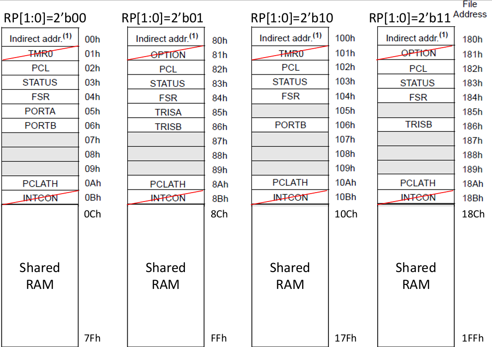
Code 7. Input, Output, and Register for Core Module // STATUS Register `define STATUS { IRP, RP, nTO, nPD, Z, DC, C } // IR `define IRB IR[ 9:7] `define IRK IR[ 7:0] `define IRF IR[ 6:0] `define IRA IR[10:0] // Memory Address `define A_INDF 7'b000_0000 `define A_PCL 7'b000_0010 module pic16core ( CLK, RST, RA, RB ); input CLK; input RST; inout [7:0] RA; inout [7:0] RB; parameter PROG = "program.mem"; // Special Register reg IRP; reg [1:0] RP; reg nTO, nPD, Z, DC, C; // 03 83 // STATUS reg [7:0] FSR; // 04 84 reg [7:0] PORTA, TRISA; // 05 85 reg [7:0] PORTB, TRISB; // 06 86 reg [4:0] PCLATH; // 0A 8A reg [7:0] RAM[ 12 : 127 ]; // 0C-7F // DATA bus reg [7:0] SDATA; // for special register reg [7:0] RDATA; // for ALU operand wire [7:0] WDATA; // for ALU result wire [7:0] DDATA; // for Data RAM Read Data // Flag data from ALU to Flag register wire CO, DCO, ZO; // Control Signal reg NOP_S; // Fetch cancel on CALL, GOTO reg [4:0] ALU_CB; // ALU control reg W_W; // Write enable for W register reg C_W, DC_W, Z_W; // Write enable for Flag register (STATUS[2:0]) reg F_W; // Write enable for Data memory reg WDT_C; // WDT clear reg nTO_S, nTO_C; // nTO set and clear reg nPD_S, nPD_C; // nPD set and clear reg SLEEP; // Sleep mode reg SLP_S; // Sleep mode set // Register reg [12:0] PC; // Program Counter { PCH, PCL } reg [13:0] IR; // Instruction Register // Register reg [12:0] PC; // Program Counter { PCH, PCL } reg [13:0] IR; // Instruction Register 2.3 Effective Addressing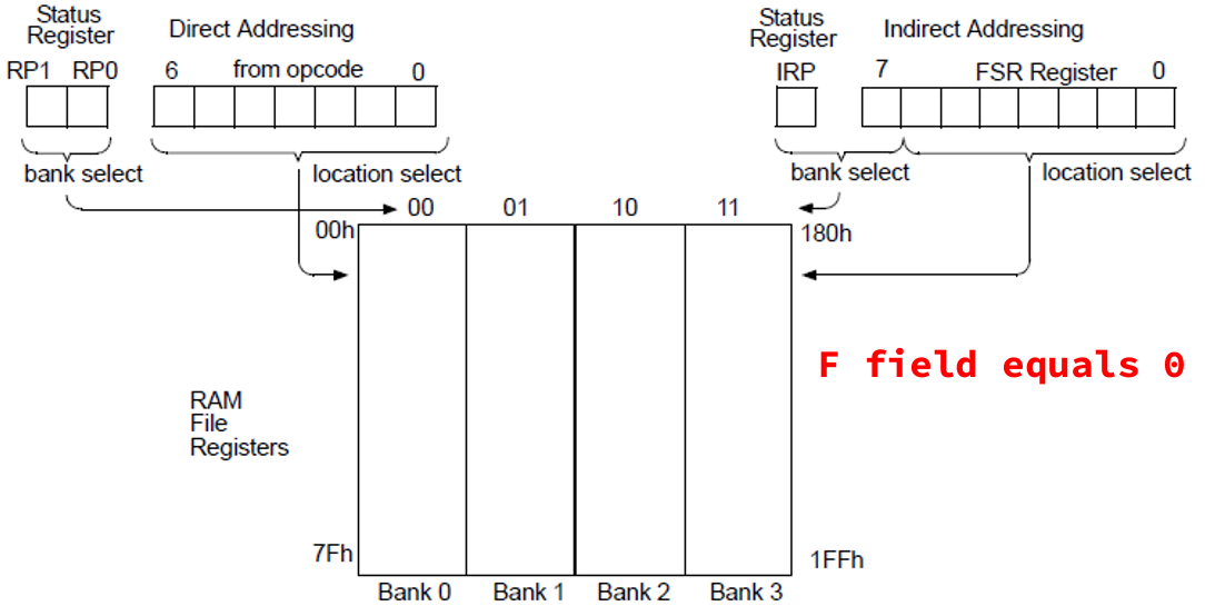
Based on Figure 5, Code 8 should write to RP if direct addressing, otherwise if indirect addressing IRP should be FSR. Code 8. Affective addressing for core module // Effective Address wire [ 8 : 0 ] EA; assign EA = ( `IRF == 0 ) ? { IRP , FSR [7:0] } : { RP , `IRF}; 2.4 Program Counter and Return Stack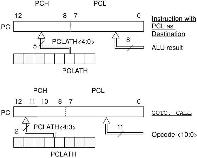 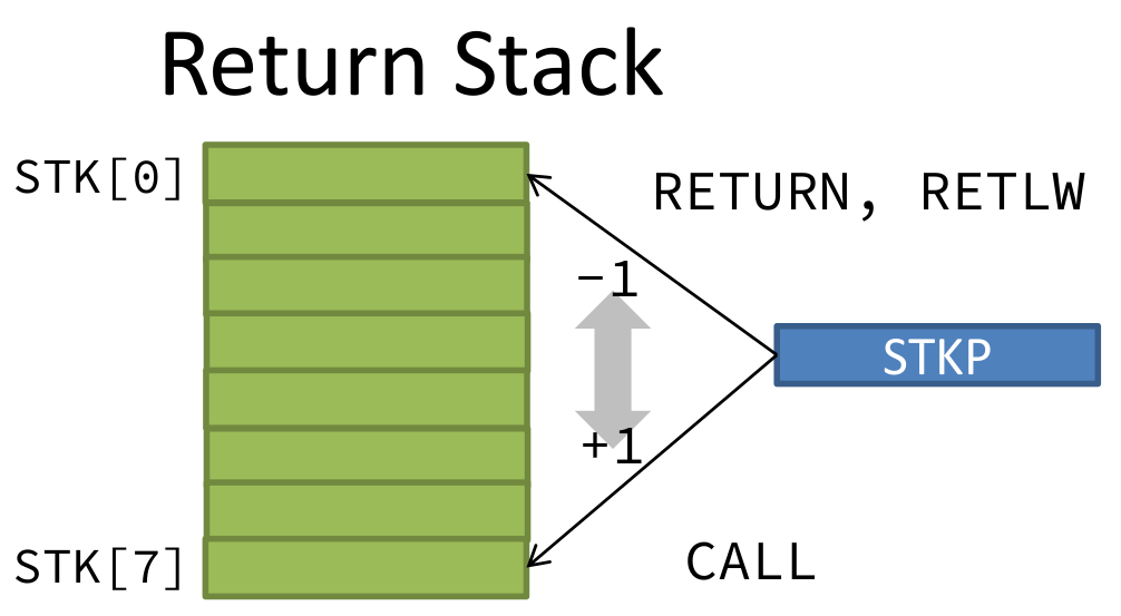
For Code 9 about program counter and return stack, the value of PC is based the left diagram of Figure 6. When operation call, then the stack is pushed, and when operation return, then the stack is popped. The value of STKP should be based on the right diagram of Figure 6. Code 9. Program counter and return stack // Program Counter & Return Stack reg [ 12:8 ] STK[0:7]; // Return Stack depth 8 reg [ 2:0] STKP; // Return stack pointer 4 bit reg STK_PU; // Stack Push enable reg STK_PO; // Stack Pop enable reg PC_W; // Write enable for CALL, GOTO // Program Counter always @( posedge CLK ) if( RST ) PC <= 0; else // RESET if( PC_W ) PC <= {PCLATH[4:3],IR[10:0] }; else // CALL, GOTO if( F_W && EA [6:0] == `A_PCL ) PC <= { PCLATH[4:3], WDATA[7:0] }; else // write PCL register if( STK_PO ) PC <= STK[ STKP-1 ]; else // RETURN, RETLW if( SLEEP || SLP_S ) PC <= PC ; else // SLEEP mode PC <= PC + 1; // Return Stack always @( posedge CLK ) begin if( RST ) STKP<= 0 ; else // for Empty if( STK_PU ) begin STK[ STKP ] <= PC ; STKP<= STKP+1; end else // for CALL if( STK_PO ) STKP<= STKP-1; // for RETxx end 2.5 Instruction Memory and Register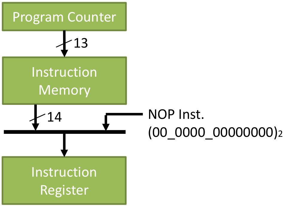 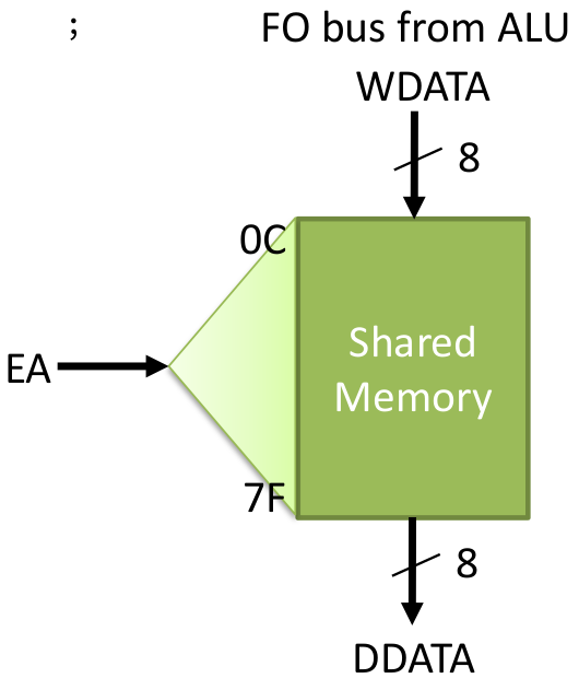
Code 10. Instruction memory and Register // Instruction Memory (8k word) reg [ 13 : 0 ] IMEM[ 0 : 8195 ]; initial begin $readmemh( PROG, IMEM ); end // Instruction Register always @( posedge CLK ) if( NOP_S || PC_W || STK_PO || RST ) IR <= 14'b00_0000_0000_0000 ; else // if CALL, RET, cond.SKIP IR <= IMEM[PC] ; // Instruction fetch 2.6 Decode and ControlTo write Code 11, the instruction table and instruction details on the datasheet [3] should be referred. Code 11 is written starting from first two bits of the instructions then the next 4 bits of the instructions. Refer again to the datasheet [3] of which status are affected. Unfortunately, sleep here is a repeat NOP. Code 11. Decode and control // Decode & Control always @( IR or ZO ) begin ALU_CB=IR[ 12 : 8 ]; F_W=0; W_W=0; Z_W=0; DC_W=0; C_W=0; nTO_S=0; nTO_C=0; nPD_S=0; nPD_C=0; STK_PU=0; STK_PO=0; NOP_S=0; PC_W=0; WDT_C=0; SLP_S=0; case( IR[ 13 : 12] ) 2'b00 : begin W_W = ~IR[7] && IR[11:8] != 4'b0000 ; F_W = IR[7]; //same with W_W = IR[7] && |IR[11:8] meaning bit 8 is 1 and bit 9-12 isn`t 0 case( IR[ 11 : 8 ] ) 4'b0000: case( IR[7] ) 1'b0: case( IR[ 6 : 0 ] ) 7'b000_1000 : begin NOP_S=1 ; STK_PO=1 ; end // RETURN // 7'b000_1001: ; // RETFIE 7'b110_0011 : begin nTO_S=1; nPD_S=1; WDT_C=1; SLP_S=1 ; NOP_S=1 ; end // SLEEP // 7'b110_0100: ; // CLRWDT default: ; // NOP endcase 1'b1: ; // MOVWF f endcase 4'b0001: begin Z_W=1 ; end // CLRW, CLRF 4'b0010: begin C_W=1 ; DC_W=1 ; Z_W=1 ; end // SUBWF 4'b0011: begin Z_W=1 ; end // DECF 4'b0100: begin Z_W=1 ; end // IORWF 4'b0101: begin Z_W=1 ; end // ANDWF 4'b0110: begin Z_W=1 ; end // XORWF 4'b0111: begin C_W=1 ; DC_W=1 ; Z_W=1 ; end // ADDWF 4'b1000: begin Z_W=1 ; end // MOVF 4'b1001: begin Z_W=1 ; end // COMF 4'b1010: begin Z_W=1 ; end // INCF 4'b1011: begin NOP_S= (ZO==1) ? 1 : 0 ; end // DECFSZ 4'b1100: begin C_W=1 ; end // RRF 4'b1101: begin C_W=1 ; end // RLF 4'b1110: ; // SWPF 4'b1111: begin NOP_S=ZO ; end // INCFSZ endcase //IR end 2'b01 : begin case( IR[ 11 : 10 ] ) 2'b00 : F_W = 1 ; // BCF f, b 2'b01 : F_W = 1 ; // BSF f, b 2'b10 : NOP_S=ZO ; // BTFSC f, b 2'b11 : NOP_S=~ZO ; // BTFSS f, b endcase end 2'b10 : begin PC_W = 1 ; NOP_S = 1 ; case( IR[ 11 ] ) 1'b0 : STK_PU = 1 ; // CALL 1'b1 : ; // GOTO endcase end 2'b11 : begin W_W= 1 ; casex( IR[ 11 : 8 ] ) 4'b00xx : begin ALU_CB=`IPSF ; end // MOVLW k //--> pass in ALU to W // 4'b01xx : begin ALU_CB=`IPSF ; STK_PO = 1 ; NOP_S = 1; end // RETLW k 4'b1000 : begin ALU_CB=`IOR ; Z_W = 1 ; end // IORLW k 4'b1001 : begin ALU_CB=`IAND ; Z_W = 1 ; end // ANDLW k 4'b1010 : begin ALU_CB=`IXOR ; Z_W = 1 ; end // XORLW k 4'b110x : begin ALU_CB=`ISUB ; C_W=1 ; DC_W=1 ; Z_W = 1 ; end // SUBLW k 4'b111x : begin ALU_CB=`IADD ; C_W=1 ; DC_W=1 ; Z_W = 1 ; end // ADDLW k endcase end endcase end // always @ ( IR or ZO ) 2.7 Special Register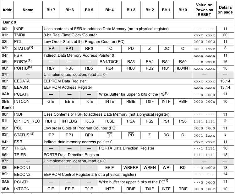
Code 12 about special register is based on Figure 3 memory map for the written bits and Figure 8 about special register itself for its values. Code 12. Special register // Special Register // Write always @( posedge CLK or posedge RST ) begin if( RST ) begin C = 0 ; DC = 0 ; Z = 0 ; IRP = 0 ; RP = 2'b00 ; nTO = 1 ; // nTO=1 on Power-on nPD = 1 ; // nPD=1 on Power-on FSR = 0 ; PCLATH = 5'b00000 ; PORTA = 8'b0000_0000 ; TRISA = 8'b1111_1111 ; // All ports for input PORTB = 8'b0000_0000 ; TRISB = 8'b1111_1111 ; // Table page 18-20 // All ports for input end else begin // STATUS if( C_W ) C = CO ; if( DC_W ) DC = DCO ; if( Z_W ) Z = ZO ; if( nPD_S ) nPD = 1'b1; if( nPD_C ) nPD = 1'b0; if( nTO_S ) nTO = 1'b1; if( nTO_C ) nTO = 1'b0; // Register Write if( F_W ) //pic16_behaviour page 41 casex( EA ) //effective address // 9'b?0_000_0001: TMR0 = WDATA; // 01 101 Described TMR0 part //find in address table // 9'b?1_000_0001:`OPTION = WDATA; // 81 181 // 9'b??_000_0010: PCL = WDATA; // 02 82 102 182 Described PC part 9'b??_000_0011:`STATUS = WDATA; // 03 83 103 183 9'b??_000_0100: FSR = WDATA; // 04 84 104 184 9'b00_000_0101: PORTA = WDATA; // 05 9'b01_000_0101: TRISA = WDATA; // 85 9'b?0_000_0110: PORTB = WDATA; // 06 106 9'b?1_000_0110: TRISB = WDATA; // 86 186 // 9'b??_000_0111: ; // 07 // 9'b??_000_1000: ; // 08 EEDATA not implement // 9'b??_000_1001: ; // 09 EEADR not implement 9'b??_000_1010: PCLATH = WDATA[4:0]; // 0A 8A 10A 18A // 9'b??_000_1011:`INTCON = WDATA; // 0B 8B 10B 18B endcase end end Code 13. Data RAM // Data RAM (Write) always @( posedge CLK ) begin if( F_W && ( EA[6:0] >= 7'b001_1000 ) ) RAM[ EA[6:0] ] <= WDATA ; //12-127 PIC16 behaviour p.46 //light behaviour p.41 //Effective Address only 7bit not 9bit start from 12 //store RAM to WDATA end // Selecter for Special Register always @( IR or PC or EA or IRP or RP or nTO or nPD or Z or DC or C // STATUS or FSR or RA or TRISA or RB or TRISB or PCLATH ) casex( EA ) // 9'b?0_000_0001: SDATA = TMR0; // 9'b?1_000_0001: SDATA =`OPTION; 9'b??_000_0010: SDATA = PC[7:0] ; // PCL 9'b??_000_0011: SDATA =`STATUS ; // STATUS 9'b??_000_0100: SDATA = FSR ; // FSR 9'b00_000_0101: SDATA = PORTA ; // RA 9'b01_000_0101: SDATA = TRISA ; // TRISA 9'b?0_000_0110: SDATA = PORTB ; // RB 9'b?1_000_0110: SDATA = TRISB ; // TRISB 9'b??_000_1010: SDATA = {3'b000, PCLATH }; // PCLATH //because SDATA is 9 bit and PCLATH is only 6 bit, we need to add 3 bit before PCLATH // 9'b??_000_1011: SDATA =`INTCON; default: SDATA = 8'bxxxx_xxxx; endcase // Data RAM Read assign DDATA = RAM[EA[7:0]] ; 2.8 Data Path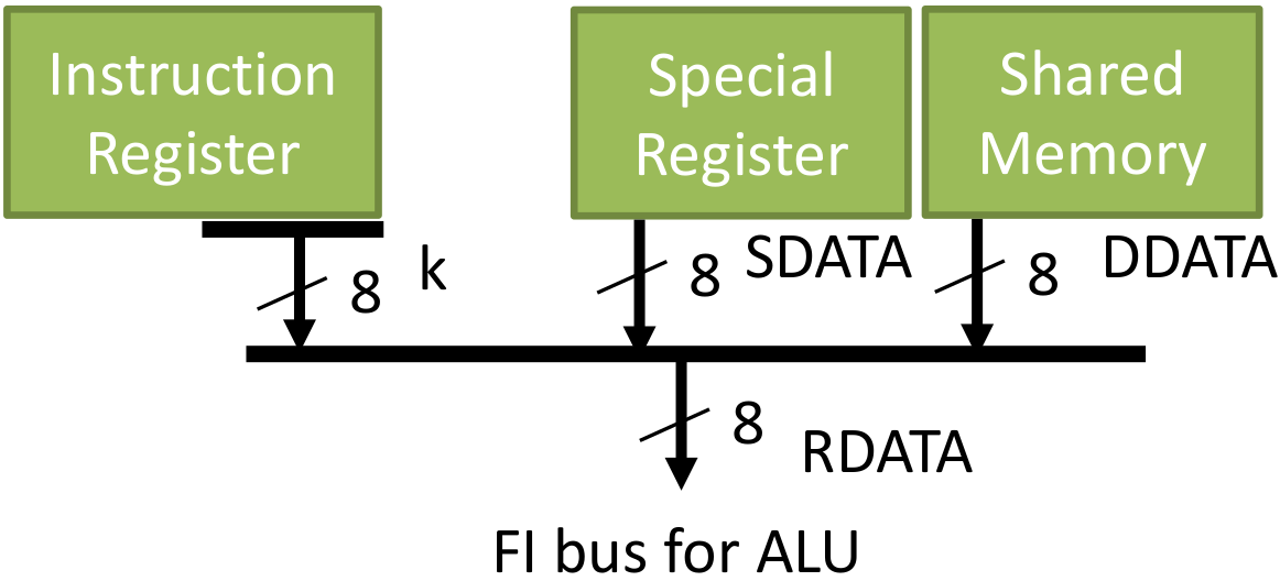
Code 14. Data selector for ALU // Data selector for ALU operand always @( IR or EA or DDATA or SDATA ) begin RDATA <= 8'bxxxx_xxxx ; if( &IR[13:12] ) RDATA <= `IRK ; else // casex( EA ) 9'b??_000_0010: RDATA <= SDATA ; // PCL 9'b??_000_0011: RDATA <= SDATA ; // STATUS 9'b??_000_0100: RDATA <= SDATA ; // FSR 9'b0?_000_0101: RDATA <= SDATA ; // PORTA, TRISA 9'b0?_000_0110: RDATA <= SDATA ; // PORTB, TRISB 9'b??_000_1010: RDATA <= SDATA ; // PCLATH default: RDATA <= RAM[EA[7:0]] ; // Shared memory endcase end 2.9 ALU Initiate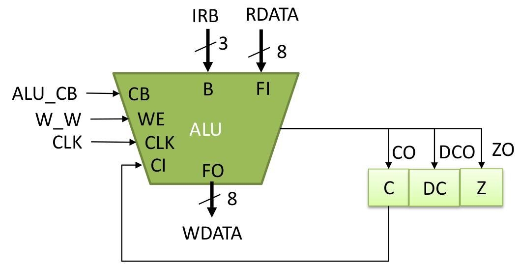
Code 15. ALU initiate code // Execute alu i_alu ( .CLK(CLK), .CB(ALU_CB), .WE(W_W), .B(`IRB), .FI(RDATA), .FO(WDATA), .CI(C), .CO(CO), .DC(DCO), .Z(ZO) ); 2.10 SleepBack on Code 11, sleep is a repeat NOP. Here on Figure 9, waking up from sleep is not implemented, sleep forever but can be reset. 
Code 16. Sleep implementation // Sleep mode always @( posedge CLK or posedge RST ) begin if(RST) SLEEP <= 0; else //0 mean run if(SLP_S) SLEEP <= 1; //1 mean execute the sleep mode end 2.11 Tristate Buffer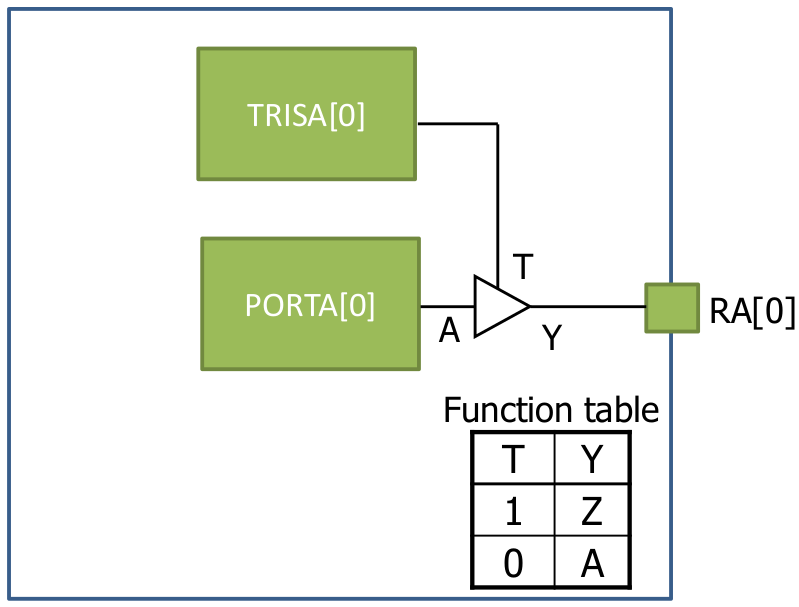
Code 17. Tristate buffer implementation // Tristate buffer for GPIO assign RA[0] = ( TRISA[0] ) ? 1'bZ : PORTA[0]; assign RA[1] = ( TRISA[1] ) ? 1'bZ : PORTA[1]; assign RA[2] = ( TRISA[2] ) ? 1'bZ : PORTA[2]; assign RA[3] = ( TRISA[3] ) ? 1'bZ : PORTA[3]; assign RA[4] = ( TRISA[4] ) ? 1'bZ : PORTA[4]; assign RA[5] = ( TRISA[5] ) ? 1'bZ : PORTA[5]; assign RA[6] = ( TRISA[6] ) ? 1'bZ : PORTA[6]; assign RA[7] = ( TRISA[7] ) ? 1'bZ : PORTA[7]; assign RB[0] = ( TRISB[0] ) ? 1'bZ : PORTB[0]; assign RB[1] = ( TRISB[1] ) ? 1'bZ : PORTB[1]; assign RB[2] = ( TRISB[2] ) ? 1'bZ : PORTB[2]; assign RB[3] = ( TRISB[3] ) ? 1'bZ : PORTB[3]; assign RB[4] = ( TRISB[4] ) ? 1'bZ : PORTB[4]; assign RB[5] = ( TRISB[5] ) ? 1'bZ : PORTB[5]; assign RB[6] = ( TRISB[6] ) ? 1'bZ : PORTB[6]; assign RB[7] = ( TRISB[7] ) ? 1'bZ : PORTB[7]; endmodule 3. Simulation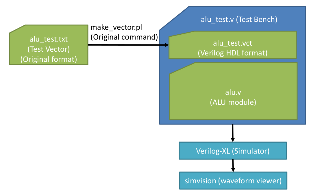

All the codes to conduct the simulation are available online [4]. For solely testing the ALU, follow Figure 13 which are about generating the clock, and testing operations starting from PASSF, subtraction, until bit test. Figure 13 compiles the test sequence from text format into verilog HDL format using make_vector.pl binary. Then these files including Code 1-6 is compiled using verilog binary. The waves can be examined using simvision which can be shown on Figure 14. All the wave values are shown in hexadecimals. CB shows the executed operation. It is seen the W register becomes 1 when performed an increment operation, and reduced to 0 when subtract operation was performed, note that HC and CO has started to become affected. After that is logical operation where the result can be seen on FO as well. In the ends of this simulation is where the bit manipulation operations are performed where the B and bitmask variables are affected. 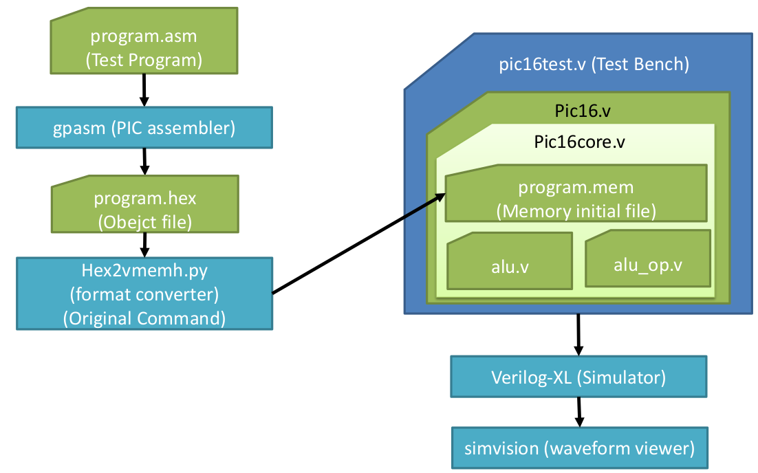
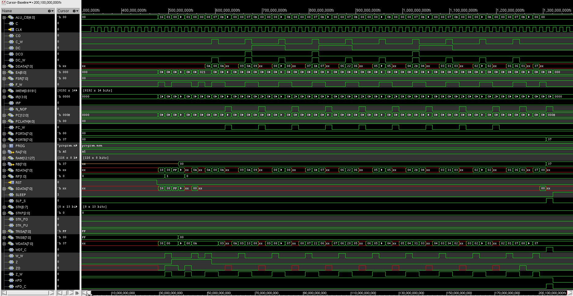
Figure 15 shows the diagram of testing the PIC16 core. The program.asm shows that only 10 operations are tested [4]. Next it have to be converted into an assembly file using gpasm which then the format have to be converted. After that the PIC16 core whole files [4] can be compiled using verilog and the waves can be seen using simvision on Figure 16. The first part of the test should bitset the RP, clear W, set TRISB to 00h, bitclear RP. The next operations are to do ten times addition of ten. DData, RData, and WData should look consistent. First the value should be 0A which is hexadecimal of 10, then it should increase to 1B and everytime added by 10. Note that the decrements are also shown from 0A until 01. In the end the result is 37 and will be transferred to PORTB. The last operation is sleep. Note that the design on this report does not implement everything from the original as shown on Table 1. Table 1. Original PIC16 versus this report’s design
4. ImplementationThe verilog HDL codes can be implemented in FPGA. On this report Nexys4 DDR board is used on Figure 17 and Vivado software is used to synthesize the code. The LED should show 110111(2) which is 37 that is the result of the addition. 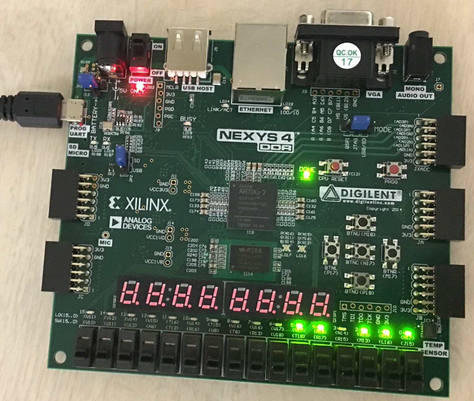
5. Reference
0 Comments
Leave a Reply. |
Archives
August 2022
Categories
All
source code
old source code Get any amount of 0FP0EXP tokens to stop automatic JavaScript Mining or get 10 0FP0EXP tokens to remove this completely. get 30 0FP0EXP Token to remove this paypal donation. get 20 0FP0EXP Token to remove my personal ADS. Get 50 0FP0EXP Token to remove my NFTS advertisements! |
 RSS Feed

